
Neuromorphic and Cognitive Integrated Circuits
Our group has made progress towards realizing Bio-inspired Neuromorphic and Cognitive Systems-on-a-Chip (SoCs) that will introduce a new paradigm for massively-parallel and event-driven computing platforms to transcend the limitations of traditional computing architecture in nano-scale CMOS technologies. We are building chips that perform pattern recognition with complexity an order of magnitude higher than traditional computing and signal processing architectures, and at power levels orders of magnitude lower than in traditional von Neumann computers.
In 2015, U. S. Office of Science and Technology (OSTP) announced a grand challenge that addresses three priorities- the National Nanotechnology Initiative, the National Strategic Computing Initiative (NSCI), and the BRAIN initiative to Create a new type of computer that can proactively interpret and learn from data, solve unfamiliar problems using what it has learned, and operate with the energy efficiency of the human brain. In alignment with this goal, our research goal is to dramatically improve computing system performance by orders of magnitude in capability and energy-efficiency, by breaking the processor-memory throughput bottleneck in von Neumann computers.
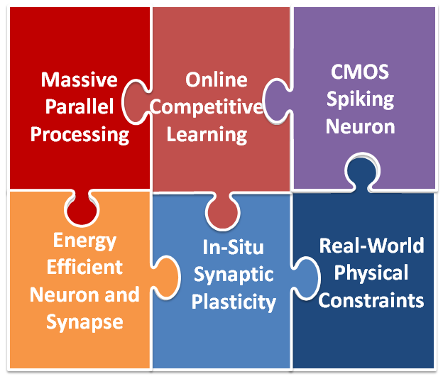
To realize neural-inspired computing, we are investigating circuit architectures for adaptive Machine Learning algorithms developed by the computational Neuroscience community. This is achieved by a large organization of mixed-signal circuit motifs comprised of event driven and energy efficient silicon neurons and a dense fabric of compact synapses integrated on CMOS chips. Our present research focus in this area include the following synergistic efforts:
CMOS-based Memristor and Synapses
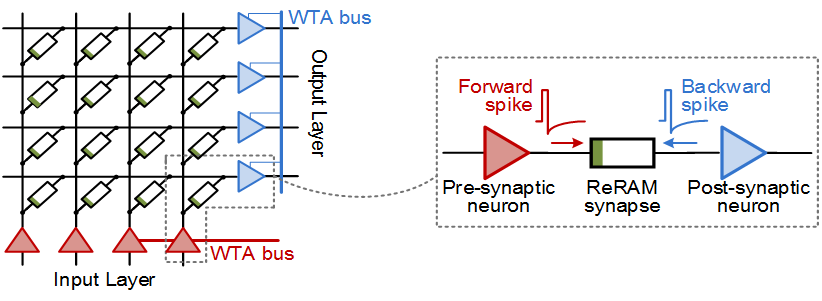
Design of transistor-based synapses with small layout footprint, biologically compatible plasticity rules and dense-integration in a nano-CMOS process with power consumption in the pJ range. We introduced the first CMOS Memristor and Memcapacitor and pioneered their use to form two-terminal Resistive/Capacitive Synapses in 2014 in our US patent disclosure. These set of inventions allow integrated circuit (IC) designers to design, fabricate, and test novel cognitive system design concepts while the 'memristor,' or resistive memory (RRAM) devices become mature and their characteristics are well understood. Further, these two-terminal CMOS synapses are a unique departure from the unidirectional conductance-based synapses in prior literature, where a MOSFET in Triode region emulates a variable conductance synapse to realize CMOS-based Dynamic synapses. These concepts thus allow designers to build CMOS neurons and synapses on the same chip, without costly process changes, and thus allow investigation of crossbar-based neuromorphic architectures.
Energy-efficient CMOS Neurons
We have demonstrated energy-efficient and compact neurons to drive dense synaptic arrays in nanoscale technologies for achieving neuron density greater than thousands of neurons on a single CMOS chip. A Neuromorphic test chip with spiking neurons and backend resistive memory, fabricated in 180-nm CMOS was demonstrated in 2014.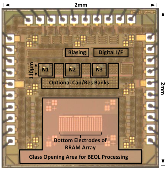
- Xinyu Wu, Vishal Saxena, Kehan Zhu, and Sakkarapani Balagopal. "A CMOS spiking neuron for brain-inspired neural networks with resistive synapses and in situ learning." IEEE Transactions on Circuits and Systems II: Express Briefs 62, no. 11 (2015): 1088-1092.
- Xinyu Wu, Vishal Saxena, and Kehan Zhu. "Homogeneous spiking neuromorphic system for real-world pattern recognition," IEEE Journal on Emerging and Selected Topics in Circuits and Systems 5.2 (2015): 254-266. (Listed in JETCAS Popular Articles, 2015).
- Xinyu Wu, Vishal Saxena, and Kehan Zhu. "A CMOS spiking neuron for dense memristor-synapse connectivity for brain-inspired computing ," IEEE International Joint Conference on Neural Networks (IJCNN), 2015.
- Xinyu Wu, Vishal Saxena, et al. "Energy-efficient STDP-based learning circuits with memristor synapses." SPIE Sensing Technology+ Applications, 2014.
Spike-based Learning Motifs using CMOS and Emerging Devices
 We are investigating several challenges in emergent and supervised learning of spiking neural-networks, realizing higher-level cognition and translation of emerging neural-inspired machine learning algorithms into chip scale systems with minimum circuit area and power overhead. A part of this effort was showcased in Prof. Saxena's recent talk at the Neuromorphic Computing Workshop at the Oak Ridge National Laboratory in July 2016. We are the first group to introduce bio-plausible multi-bit STDP plasticity using dendrites with bistable stochastic RRAM/memristive devices. This invention paves the path towards practical realization of spiking deep-learning architectures using realistic behavior of emerging memory/memristive devices.
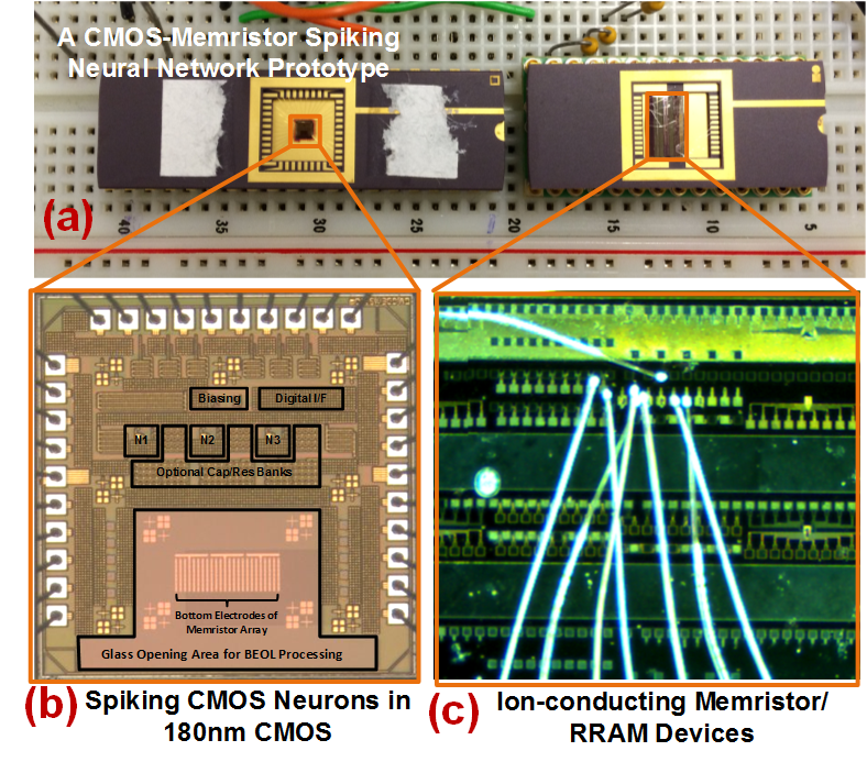
The image on the right shows the neuromorphic test chip with spiking neurons integrated with CBRAM synapses (courtesy Prof. Maria Mitkova of Boise State).
We are investigating several challenges in emergent and supervised learning of spiking neural-networks, realizing higher-level cognition and translation of emerging neural-inspired machine learning algorithms into chip scale systems with minimum circuit area and power overhead. A part of this effort was showcased in Prof. Saxena's recent talk at the Neuromorphic Computing Workshop at the Oak Ridge National Laboratory in July 2016. We are the first group to introduce bio-plausible multi-bit STDP plasticity using dendrites with bistable stochastic RRAM/memristive devices. This invention paves the path towards practical realization of spiking deep-learning architectures using realistic behavior of emerging memory/memristive devices.
The image on the right shows the neuromorphic test chip with spiking neurons integrated with CBRAM synapses (courtesy Prof. Maria Mitkova of Boise State).
- Xinyu Wu and Vishal Saxena "Enabling Bio-Plausible Multi-level STDP using CMOS Neurons with Dendrites and Bistable RRAMs," arXiv:1612.01491.
- Xinyu Wu, Vishal Saxena, and Kehan Zhu, "Homogeneous spiking neuromorphic system for real-world pattern recognition," IEEE Journal on Emerging and Selected Topics in Circuits and Systems 5.2 (2015): 254-266. (Listed in JETCAS Popular Articles, 2015).
- Vishal Saxena, Xinyu Wu, and Maria Mitkova, "Addressing challenges in neuromorphic computing with memristive synapses,", Neuromorphic Computing Workshop, 2016.
Algorithm Development for Neuromorphic Hardware
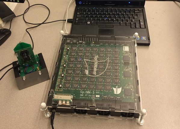 Our group collaborates with several experts in Machine Learning, Controls, Computational Neuroscience, and Signal Processing areas to develop spike-base computing algorithms using Neuromorphic platforms. These massively-parallel, spike-based computing platforms include the SpiNNaker system from the EU Brain Project, and IBM TrueNorth processor which resulted from the DARPA SYNAPSE program. The image on the right shows the SpiNNaker Neurmorphic computing platform interfaced with eDVS or silicon retina from IniLabs (courtesy Prof. John Chiasson of Boise State), which serves as one of the prototyping platform for our Neuromorphic Computing research.
Energy-efficient AER Interconnects
We are also investigating ultra low-power interconnects for event-driven (AER) communication for a large network of neuromorphic computing cores.While being successfully demonstrated, the proposed cognitive computing architectures will realize a massively parallel, highly scalable and energy-efficient event-driven intelligent signal processing (ISP) platform to tackle complex real-time machine learning tasks such as pattern recognition, robotic control, visual pattern and motion detection and brain-machine interfaces with power consumption comparable to biological brains.