The Analog Mixed Signal and Photonic IC (AMPIC) Laboratory is directed by Dr. Vishal Saxena. The Lab is equipped with state of the art workstations and instruments for Analog, Mixed-Signal and Photonic Integrated Circuit design and testing. The AMS lab also houses the Linux server cluster supporting the Cadence and Synopsys tools for research and teaching activities.
Current Research Focus
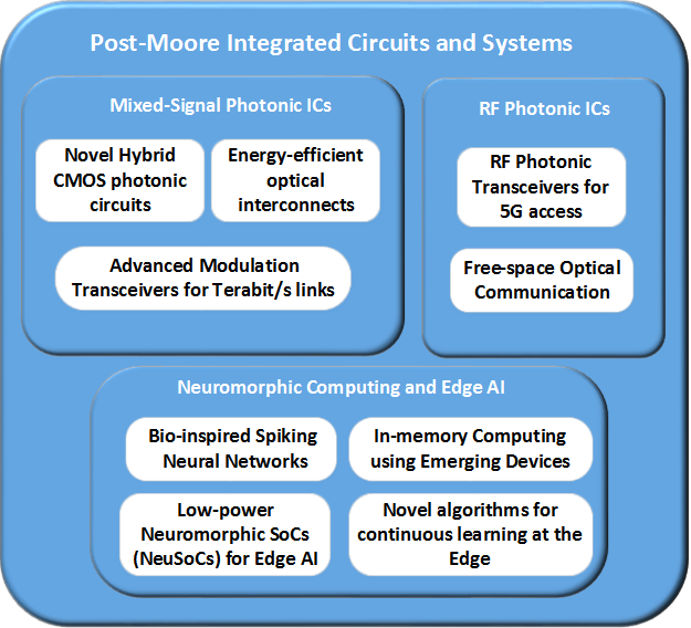 Presently integrated circuits (IC) and systems research and Semiconductor industry are at an inflection point where it faces three key challenges - (1) sustainability of the decades long trend of performance gain through Moore’s scaling, (2) lack of scalability of current computing and data communication architectures to tackle Artificial Intelligence (AI) and Big Data applications while consuming lower energy, and (3) traditional mixed-signal and RF IC architectures have largely matured and need infusion of new ideas for growth. These challenges present opportunities to IC designers to explore integration of beyond-CMOS technologies such as silicon photonics, emerging devices, and exploitation of machine learning and neuromorphic approaches to realize system-level innovation and improved energy-efficiency. My current research pursues these challenges through the following efforts:
Current Research
- High-speed energy-efficient microring-modulator based optical transceivers
- Electronic Photonic AI Accelerators
- Programmable Photonic ICs`
- RF Photonic ICs for Spectrum Awareness
- Photonic IC exploration with Phase-change, TFLN, and other devices
- Mixed-signal Computing Circuits for low-power AI and Neuromorphic Computing
- Agentic AI for Analog IC Design