
Electronic Photonic Integrated Circuits (EPIC)
Profusion of network intensive applications such as cloud computing, social media, high-definition multimedia streaming have resulted in a rapid upward scaling in data rates at all levels of system hierarchy. Conventional electrical signaling over copper channels is severely limited by attenuation, dispersion and crosstalk resulting in poor scaling beyond 10 Gbps rates. At the same time advances in next-generation wireless (5G and beyond) necessitate wider data pipes in the infrastructure and access networks.
To alleviate these bottlenecks, AMPIC group's research is focused on Harnessing Light to Transform IC Design in the post-Moore's scaling era. Specifically, we developed mixed-signal and RF photonics integrated circuits which employ photons in a guided medium, instead of electrons. Challenges involve modeling of photonic components for system-level design and simulation, high-speed mixed signal and mmWave circuit design, packaging and testing of hybrid CMOS photonics systems. Also, such circuits must be adaptively tuned in the presence of process, voltage and temperature (PVT-) dependent variations in the photonic components. My research group performs design of photonics and mixed-signal (Bi)CMOS chips, fabrication through semiconductor foundries located globally, integration into a 3D packaged system followed by hardware prototyping and test.
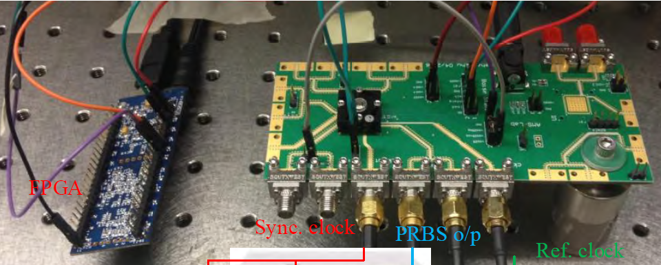
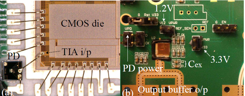
Further, in order to exploit photonics beyond binary interconnects, novel interfaces for analog data conversion and processing are needed. Research outcomes will empower integrated circuit researchers by equipping them with a new photonics expertise to take on design challenges in a nano-scaled technologies, where data transfer bottlenecks constrain system performance. Experimental results for the receiver demonstrate over 40 Gbps binary data rate with energy-efficiency comparable to the state-of-the-art. To test these hybrid chips, state-of-the-art optoelectronic probe and test setup has been assembled. Further, AMPIC group has initiated development of compact models for silicon photonics components using foundry device data. A direct application of these mixed-signal photonic circuits is in single-wavelength advanced modulation optical interconnects. The interconnects include on-chip, chip-to-chip, and data center ommunication.
The RF photonic component of the research focuses on use of photonics for high-bandwdith signal processing to alleviate challenges with the electronics-only solutions. Potential applications of this technology will result in photonic-enabled RF and mm-wave communication, free-space optical links, compact RADAR/LIDARs.
Current Research
- High-speed energy-efficient microring-modulator based transmitters
- Photonic IC exploration with Phase-change, TFLN, and other devices
- RF Photonic ICs for Spectrum Awareness
- Electronic Photonic AI Accelerators
- Neuromorphic Computing Circuits and low-power AI