NSF FuSERF Photonic Channelizer
Collaborator 2: Prof. Francesco Restuccia, PI, Northeastern University
Collaborator 3: Prof. Jia Di, University of Arkansas, PI
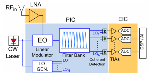
This interdisciplinary NSF FuSE project investigates the co-design and integration of photonic integrated circuits (PICs) with mixed-signal CMOS electronic ICs (EICs) to realize an RF photonic channelizer for real-time wideband RF spectrum perception and processing. The AMPIC group at the University of Delaware is responsible for the design of the photonic and electronic chiplets. Collaborating teams contribute DSP and AI algorithm development and digital ASIC design. The complete system interfaces with an AMD Xilinx RFSoC FPGA platform for digital back-end processing.
The system employs a discrete electro-optic modulator to convert RF signals into the optical domain. The modulated optical signal is then processed through the RF channelizer PIC, and the channelized outputs are routed through the CMOS TIA EIC to on-board ADCs for digital processing.
Project Goals
- Design, fabricate, and experimentally validate a foundry-processed PIC front-end capable of channelizing a wide RF bandwidth using passive optical filter architectures with strong adjacent-channel isolation.
- Design, fabricate, and test a CMOS mixed-signal EIC with high-linearity transimpedance amplifiers (TIAs) to interface PIC photodetector outputs with downstream ADCs on the FPGA board.
- Co-package and system-level validate the PIC and EIC chiplets alongside the FPGA-based digital back-end to demonstrate complete channelizer functionality.
Project Highlights
PIC Test Chip Characterization
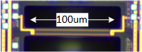
A test PIC fabricated during Year 1 was fully characterized in Year 2. The chip contained photonic building blocks including low-loss broadband optical couplers, thermo-optic phase shifters with substrate undercut heaters, and combined test structures. Experimental results have been published in CLEO 2026, with others to follow.
Photonic IC Design & Tape-Out
An 8-channel RF photonic channelizer was designed using a passive optical filter architecture, overcoming significant layout challenges by leveraging an ultra-low-loss foundry process to fit the required waveguide lengths on chip. This first-of-its-kind design was submitted for fabrication through a multi-project wafer run.
CMOS Electronic IC Design
A linear TIA chain was designed in a leading-edge CMOS process to interface the photonic chip's outputs with the ADCs, featuring a resistive-feedback topology, programmable gain, and DC offset cancellation. Preliminary simulations confirm all key specifications, with the TIA and PIC co-designed to ensure compatibility for future system integration.
Publications
-
PublishedMoussa, A. and Saxena, V., "A Hybrid CMOS Photonic RF Channelizer: System Design and Analysis," Proc. IEEE International Midwest Conference on Circuits and Systems (MWSCAS), 2025, East Lansing, MI.
-
PublishedSaxena, V. and Moussa, A., "CMOS-RRAM Neuromorphic Accelerators Using Multi-bit Neurons," Proc. IEEE International Midwest Conference on Circuits and Systems (MWSCAS), 2025, East Lansing, MI.
-
PublishedAfsary, N. and Saxena, V., "CMOS-Compatible Thermo-Optic Switch with Undercut Resistive Heater," Conf. on Lasers and Electro-Optics (CLEO), IEEE/Optica, 2026.