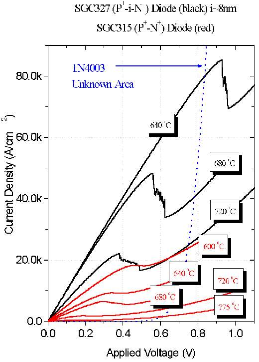
The objective is to fabricate and characterize light emitters and lasers that are fabricated from germanium-tin (GeSn) alloys, which will be produced by chemical vapor deposition (CVD) and by molecular beam epitaxy (MBE). GeSn materials have been grown with high quality, and their energy bandgap is tunable in the mid-infrared range by adjusting the composition during epitaxial growth. The presence of tensile strain reduces the Γ conduction band in Ge grown on SiGeSn alloys. We will determine the characteristics and limitations of light emitting devices made from these direct bandgap alloys and strained layers. Group IV materials, especially GeSn alloys, are attractive for mid-IR light emitting devices, but are not yet well understood. By fabricating GeSn devices, and evaluating their properties, we will add valuable information about the behavior of these novel alloys under device operation.
This project addresses the application of magneto-resistive sensors to detect biochemicals, including DNA and proteins. The operating principle is that magnetic particles of nanometer size are prepared as markers that tag biomolecule targets by chemical binding. A complementary probe biochemical, which specifically bonds to the sought target, is anchored to the surface of the magneto-sensors by chemical surface treatment. The magneto-sensor is placed in close proximity to a test sample of biochemicals, by micropipette. If the target molecule matches its complementary probe anchored to the sensor surface, the molecules will bind, along with their nanomagnet tags, and stay fixed to the sensor surface without being washed away. If the magneto-resistance sensor shows a change in resistance by the fringing field of the nanomagnet, the presence of that particular target is indicated. If the probe and target do not match, the target molecules get washed away with their nano-tags, and there is no change in magnetoresistance. The magneto-resistive sensors have been shown to detect a single magnetic particle of micron-size. A microwave magnetic field can precess the free magnetic layer in spin valve devices and magnetic tunnel junctions. Consequently, the magnetoresistance changes, leading to an average resistance change with respect to the initial state (parallel or antiparallel). A dc current applied through the device picks up the resistance change and converts it into an ac voltage signal which can be detected using a lock-in technique. We found that the ac voltage signal is related to the microwave power.
We are working with a small business, QuantTera, to develop silicon-germanium based quantum dot optoelectronic materials. The proposed quantum dot nanostructures operate over a wide range of optical wavelengths by virtue of their composition and size distribution are capable of exhibiting diverse controllable and predictable physical responses when subjected to various external conditions. This innovative nanomaterial will be multifunctional which would allow the development of broadly absorbing solar cells on silicon with a single junction technology for alternative energy applications or the development of highly efficient broadband photo-detectors for telecommunications applications. Using layers of silicon-germanium quantum dots that were grown by molecular beam epitaxy, we have fabricated light emitters that operate at low temperatures and up to room temperature.
Dilute nitride semiconductors have been proposed as a good choice for mid- and long-waver infrared detectors, because theoretical analysis has shown that a small amount of nitrogen in antimonide semiconductors is capable of drastically lowering the bandgap and enhancing the recombination parameters, carrier confinement, transport properties and temperature characteristics of the detector materials and devices. Thus far, the potential of dilute nitride materials has not been realized because of the challenges and difficulties of incorporation of even minute quantities of nitrogen in III-V compound semiconductors. These difficulties include achieving the optimum growth conditions, the high lattice mismatch for the material responsive to VLWIR and the high background doping. With another faculty member (Prof. Goossen), we have been working with a small business, Epitaxial Technologies, to develop dilute nitride strained layer superlattices in the design of detectors. We used semiconductor modeling software, the FemB k•p computer simulation software package from Quantum Semiconductor Algorithms, Inc (QSA), to simulate the properties of dilute nitride structures. This software uses the k•p technique for the calculation of electronic eigenstates in semiconductor quantum structures. The k•p technique is an approximation method that calculates energy versus wavevector dispersion, and wave functions in vicinity of band critical points in k space such as the point.
This project addresses the development of solar cells that are optimized for photons from the low energy part of the solar spectrum in the range between the bandgaps of germanium (0.66 eV) and silicon (1.12 eV). This is the wavelength range from 1.88 to 1.1 micrometer, where silicon is transparent. This research is important, because the germanium cells could be operated underneath silicon cells in a tandem multijunction configuration, and thus collect solar power that would otherwise be lost. The amount of power in the solar spectrum between 0.66 and 1.1 eV with “1-sun” (AM 1.5) illumination is 15 %, or about 15 milliwatts–cm-2, compared to the total illumination of 100 mW–cm-2. Of the long wave solar energy that remains after conversion by conventional silicon cells, the proposed low energy cells can add a few percent of marginal efficiency, which could be leveraged over the huge number of new solar systems, which are growing at about 48 % per year worldwide. To combine excellent performance with low cost, the proposed cells will be fabricated of silicon germanium (SiGe) alloys by the epitaxial technique of chemical vapor deposition (CVD). Silicon and germanium can intermix across the whole alloy composition range, and the net bandgap energy can vary from 0.66 to 1.12 eV, depending on the composition. By optimizing solar cells that utilize low energy photons, our research should significantly improve the efficiency of solar power systems.
This project addresses an experimental and theoretical study of the synthesis and properties of nanostructures that have multiple doped regions that are in contact with regions of different doping, in silicon-germanium (SiGe) based materials. The goal is to identify mechanisms governing the formation of nanostructures that are doped with shallow acceptors, in contact with regions having shallow donors, and the underlying transport and radiative transitions between localized and resonant states, the band continuum, and between other doped regions on the nanoscale. This research seeks to understand how the synthesis of doped SiGe nanostructures depends on interfaces, composition, strain, and neighboring dopants. Such multiple doped nanostructures can be formed during molecular beam epitaxy by interrupting growth, changing the dopant type and continuing the growth with another set of nanostructures. The impurities in nanostructures will be characterized by techniques including temperature dependent terahertz radiative emission spectroscopy, current versus voltage measurements, and atomic force microscopy. If successful, this research will give an improved understanding of dopants in nanoparticles that are surrounded by regions with different dopants, in the SiGe based materials system. This research may have important technological consequences because the understanding of doping in structures is pivotal to the operation of devices and circuits.
During the past few years, there have been studies of semiconductor devices that generate and detect frequencies from 0.3 - 10 Terahertz (1000 - 30 mm). Infrared emitters such as the Quantum Cascade Laser in III-V semiconductors have been difficult to extend to these frequencies due to the high absorption by polar phonons in the reststrahlen bands, but can produce superb results if the devices are constructed from multiple active regions [1]. In contrast, Si has no reststrahlen absorption band and therefore may be able to operate over a broader THz range and provide lower loss waveguides than the III-V semiconductors. In our group, we work on the fabrication and characterization of sources and detectors based on SiGe nanotechnology.
Emitters based on intersubband transitions in quantum wells of III-V compounds such as the quantum cascade laser have made remarkable progress, and operation in the THz range has recently been demonstrated [2]. Similar devices based on silicon-germanium quantum wells and cascades are attractive due to possible integration with conventional silicon circuitry, and because of lower free-carrier and reststrahlen-band absorption. In the SiGe material system, the band gap difference manifests itself mainly as an offset in the valence band, and quantum well devices typically employ the confinement of holes. By making semiconductor devices with layers of Si alternating with SiGe alloys, we create quantum energy wells in the valence band. The intersubband energy levels in the quantum wells exhibit electron and hole transitions in the far infrared electromagnetic spectrum - at TeraHertz frequencies. The structures are unipolar in the sense that only one carrier type is involved in the device operation. This is unlike conventional light emitting diodes and lasers that use bipolar recombination of electrons with holes. Electroluminescence has been reported from structures based on intersubband transitions between confined states in SiGe quantum wells, however; operation has been achieved only at low output powers [3]. Hydrogenic shallow donor impurity states in bulk silicon have also been exploited for terahertz emission using optical pumping, and have garnered attention due to their simple and low-cost fabrication [4, 5].
Terahertz signals can be detected by very narrow gap semiconductor photodiodes (such as HgCdTe to a low frequency of about 20 THz), extrinsic photoconductors (such as Ge:Ga in the range from 50 to 150 um), quantum well infrared photodetectors (QWIPs), and thermal detectors including bolometers and pyroelectric detectors. Although their response respectable, there is still need to improve their temperature of operation, and their detectivity performance.
Other TeraHertz Research and Information
The major findings of this work are that doped Ge quantum dots were grown by molecular beam epitaxy and were investigated by PL and AFM. The dots produced photoluminescence in the energy range from 0.75 to 0.95 eV. Compared to the undoped dots, the boron and phosphorus dopants caused a redshift in the energy of peak emission by 60 to 80 meV, which was attributed to the decrease in number of smaller pyramid type dots with doping. The increased photoluminescence intensity with temperature indicated higher activation energy for the doped samples, suggesting changes in the probability of radiative transitions at elevated temperature, which can be important for technological applications. These findings on the materials properties of quantum dots could offer a basis for understanding the effects of dopants in quantum dots for the applications of future Ge-Si nanoscale electronic and optoelectronic devices.
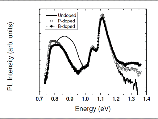
Figure. 80 K PL spectra from as-grown undoped (Sample A - SGC 520), boron (Sample B - SGC 557) and phosphorus-doped (Sample C - SGC 558) Ge quantum dots showing a red-shift for the Ge quantum dot emission peak at 62-80 meV for the doped samples relative to the undoped layers. Incident laser power was 117 mW
This work was supported by the NSF under Award Number: DMR 0601920
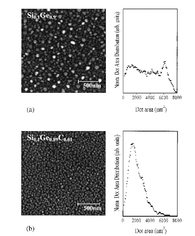
FIG. 1. (a) Atomic force microscopy scan of 2 µm x 2µm area of Si0.1Ge0.89 grown on(311) Si and quantum dot area distribution, (b) atomic force microscopy scan of 2 µm x 2µm area of Si0.1Ge0.89C0.01 grown on (311) Si and quantum dot area distribution. The Curves were normalized by multiplying the number of equally sized quantum dots with their area and dividing the result by the scan area.
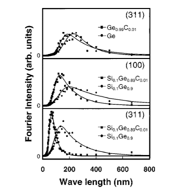
FIG. 2. Fourier intensity distribution spectrum vs. quantum dot spatial wavelength for Ge, GeC, SiGe, and SiGeC quantum dots on Si(311) and Si(001), obtained from AFM scans of Fig. 1, over the 2 µm x 2µm area. Markers represent measured data, solid lines were calculated by fitting the measured data to an exponentially altered Gaussian.
Under Construction
SiC can be alloyed with Ge, forming a new material (SiC:Ge) that may extend the opportunities for high-power, high temperature applications The structural, electronic, and optical properties of single crystalline n-type 4H-SiC implanted with Ge atoms have been investigated through x-ray diffraction (XRD), Rutherford backscattering spectroscopy (RBS), Raman spectroscopy and sheet resistivity measurements. Ge atoms are implanted under the conditions of a 300 KeV ion beam energy with a dose of 2 x 10 16 cm-2. X-ray diffraction of the Ge-implanted sample showed broadening of the Bragg peaks. A shoulder on the (0004) reflection indicated an increase in the lattice constant corresponding to Ge substitution and implantation induced lattice damage. The composition of Ge detected through XRD was reasonably consistent with RBS measurements that indicated the presence of 1.2% Ge in a 1600 Å thick layer near the SiC surface. Raman Spectroscopy showed fundamental differences in the Ge implanted SiC (SiC:Ge) compared to a pure sample of SiC. Sheet resistivity measurements indicate a higher conductivity in the Ge implant by a factor of 1.94 compared to unimplanted SiC. These results demonstrate the possibility of Ge substitution in the crystalline lattice of 4H-SiC substrates for possible electronic device applications. SiC:Ge may lead to new heterostructures that are compatible with SiC, but more work is needed.
Under Construction
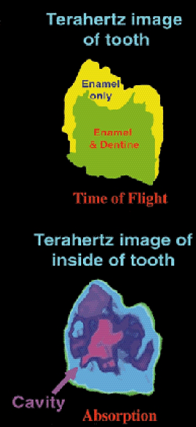
Medical applications of TeraHertz waves are being tested. They can penetrate medical tissues several cm returning an image like an x-ray used for analysis.
Picture from:
D.D. Arnone, C. Ciesla and M. Pepper
"TeraHertz imaging comes into view"
Physics World 13(4), 35-40 (April 2000)
Alumina-better known as sapphire or ruby in its mineral form-may promise faster, smaller, more reliable computer circuits, thanks to University of Delaware technology described in the July 1998 Journal of Electronic Materials, tentatively scheduled for mailing July 13. Developed by UD Electrical Engineering Prof. James Kolodzey and colleagues, a new technique produces extremely thin, alumina films offering an electrical storage capacity three times greater than silicon dioxide, the material most commonly used in existing transistors-the 'on/off' switching devices in semiconducting circuits. "We've created alumina films demonstrating a capacitance or dielectric constant of around 12, so they can hold 12 times more electrical charge than air-and roughly three times more than silicon dioxide," Kolodzey says. "If these films can be successfully integrated into a device, it may be possible to make them three times thicker, which should eliminate reliability problems." As electronic circuits continue to shrink, Kolodzey explains, electrons moving near silicon dioxide films thinner than about 3 nanometers-roughly the width of 15 atoms-often begin to "tunnel" or leak from designated pathways. Whenever tunneling occurs, circuits lose efficiency, just as a leaky cup wastes water. In addition to their enhanced electrical storage, the UD alumina films exhibited device-grade material characteristics, with relatively few current-blocking flaws found in surface regions, according to Kolodzey and his coauthors, including Johnson O. Olowolafe, UD associate professor of electrical engineering. (Net oxide-trapped-charge density was measured at ~1011 cm-2.) "Alumina films aren't going to turn your PC into a Cray supercomputer anytime soon," Kolodzey cautions. "But other researchers have predicted that circuits based on thin-film alumina transistors might be one thousand times faster at performing 'flash memory' or rapid-recall tasks." (See reference.) Generating Jewels How did Kolodzey and his colleagues grow such promising, thin alumina films? The new UD process involves indirectly or reactively sputtering aluminum onto a positively charged silicon substrate in the presence of nitrogen and argon gases, then exposing the material to air and heat. Specifically, the silicon substrate is secured on a mounting device inside a vacuum chamber, along with argon and nitrogen gas and an aluminum "target," says Kolodzey's graduate student, Thomas N. Adam. When subjected to high-voltage electricity, positively charged atom clusters or ions from the argon begin to bombard the negatively charged aluminum target. As ions pummel the target, aluminum atoms are dislodged, react with nitrogen, and then are drawn onto the silicon substrate. In addition, Adam explains, "We oxidize aluminum nitride. We basically replace the nitrogen with oxygen to form aluminum oxide, or alumina." Once coated, the substrate is placed inside a small, cylindrical furnace. Heating a sample for one hour at 800 degrees Celsius (1475 degrees Fahrenheit) produces alumina layers with a thickness of 33 nanometers, UD researchers report. Setting the temperature to 1000 degrees C (1832 degrees F) for the same period of time generates films 524 nanometers thick. Because alumina films store more electricity, Kolodzey notes, they could be made thicker than the silicon dioxide layers in existing transistors. While the UD technique requires an additional processing step to oxidize the alumina films, Kolodzey says their potential for improved reliability in semiconducting circuits should prove worthwhile. "If silicon dioxide layers within transistors become too thin, they'll eventually fail," he says. "We can't shrink existing materials much more before we're going to begin seeing significant problems." Other members of the UD research team included students Mike Dashiell, Guohua Qiu, Ralf Jonczyk and Dave Smith; as well Karl Unruh, an associate professor of physics and astronomy at UD; Charles P. Swann, a professor emeritus with the Bartol Research Institute at UD; John Suehle of the National Institute of Standards and Technology; and Yuan Chen of the Center for Reliability Engineering at the University of Maryland, College Park. Research described in this news release received support from the U.S. Army Research Office and from the Defense Advanced Research Projects Agency. * Reference-W.H. Lee, J. T. Clemens, R. C. Keller, and L. Manchanda, "A novel high K inter-poly dielectric (IPD), Al2O3 low voltage/high speed flash memories: erasing in msecs at 3.3 V.," Tech. Dig. 1997 Symp. on VLSI Technology, Feb. 1998, paper 9A-4, pp. 117-118. July 13, 1998
National Nanotechnology Initiative
Richard Feynman's Lecture: "There's Plenty of Room at the Bottom"
http://www.sciam.com/nanotech/
http://www.spectrum.ieee.org/WEBONLY/resource/sep01/ntran.html
Nanochips article in Scientific American, April 2004