
There are two major areas of research at the Integrated Photonics Systems Laboratory: Optical interconnects and optical components for concentrating photovoltaics.
Optical Interconnects
Continued reduction in CMOS critical dimensions has resulted in increasing bandwidth in the communications fabric in high performance computing (HPC) systems - and resulted in optical interconnects (OI) being deployed as ever decreasing length scales in HPC systems. Continued scaling of HPC performance to the 10 GFLOPS/W level and beyond will require OI to be integrated ever closer to the CMOS chip. In our group, we explore the use of OI at the chip level to replace the global metal interconnects that cannot keep pace with the growing on-chip bandwidth requirements. A hybrid integration scheme is examined that uses a dense arrays of multiple quantum well (MQW) modulators and photodetectors that are bonded to a silicon chip and then coupled to lithographically defined polymeric waveguides to route the optical signals.
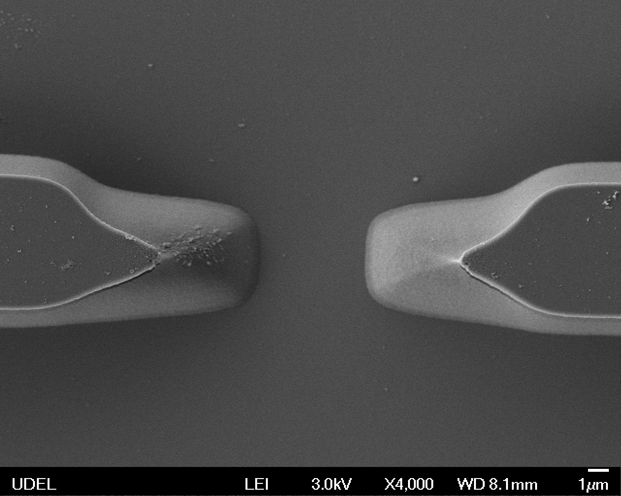
Since the problematic global interconnects are targeted for replacement, the fabrication of the CMOS level, and the associated local and intermediate metal wiring, is not affected. At the global wiring level, vias are brought up to the top level, which is planarized. These exposed vias enable subsequent flip-chip bonding of a GaAs-based MQW wafer. After bonding, the GaAs substrate is removed by chemical etching, exposing the array of MQW devices. The polymeric optical fabric is the spun on to MQW plane by first depositing and curing a thin cladding layer. The waveguide core layer is then spun on. The desired waveguiding and coupler features are then fabricated into the top layer using grayscale lithography -- in which the UV exposure dose is spatially tailored to create three dimensional structures in the top photoresist layer. This is achieved by varying the optical density across the mask. Two distinct types of small-footprint couplers are currently being explored. Both are designed to enable optical coupling from waveguides into surface-normal MQW devices. One is a curved facet coupler, shown below in (a), and the second is a prism coupler, shown below in (b).
 |
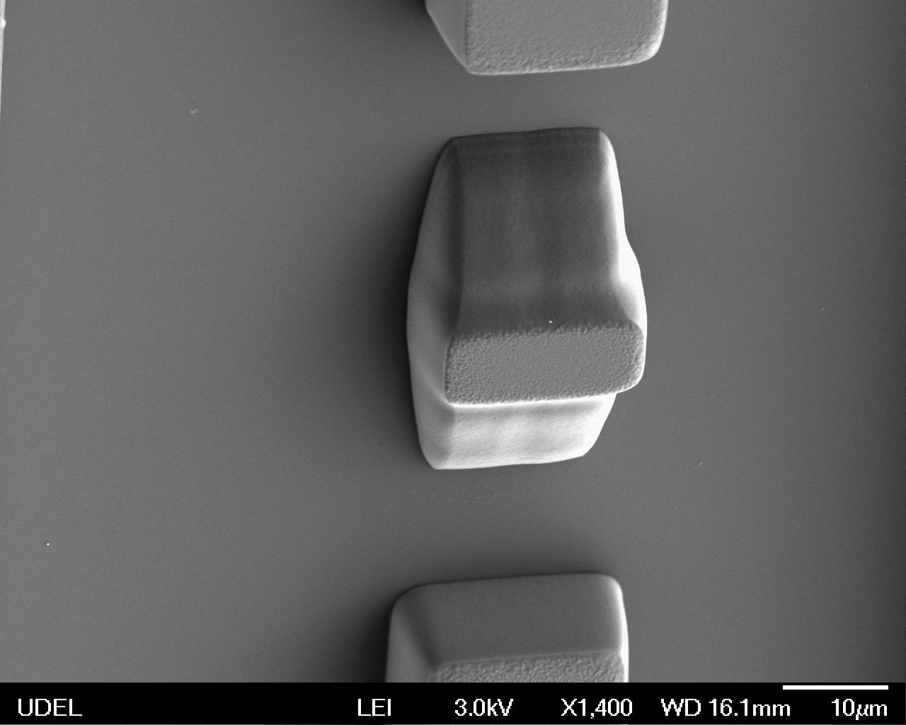 |
| (a) | (b) |
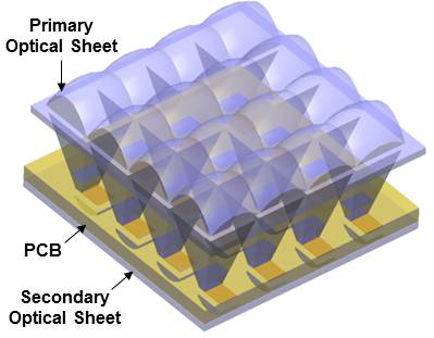
Concentrating Photovoltaics
It is well-known that using multi-band gap solar cells that effectively cover the solar spectrum in a PV system can achieve improved efficiency – and that even further efficiency improvement may be gained through concentration. Multi-junction solar cells, with different band-gap energies connected independently in a parallel structure, may indeed minimize the spectrum and material mismatches – but they also demand efficient, low-cost, and compact optical concentrating and spectrum splitting.
Novel multi-junction dispersive concentrated photovoltaic (CPV) approaches are investigated that are based on integrating optical concentration and spectrum-splitting components with pixelated spectrally selective solar cells at the "chip-scale." A key aspect is that the multi-junction cells are arranged in a lateral configuration on a common plane. The integrated optical concentrator design combines imaging and non-imaging optical elements to achieve desired levels of concentration to provide high flux transfer and prescribed irradiation patterns on multiple solar cells with different band-gap energies. Each unit cell may be contained in a volume of a few cubic centimeters or less. Figure (a) below describes the unit cell of the concentrator. A prototype is shown in Figure (b). The benefits of this concept come from the anticipated ability – using large-area fabrication techniques – to aggregate many unit cells into large tiled arrays, as shown in figure (c), that maintain a low overall geometric profile, yet reap the benefits of CPV.
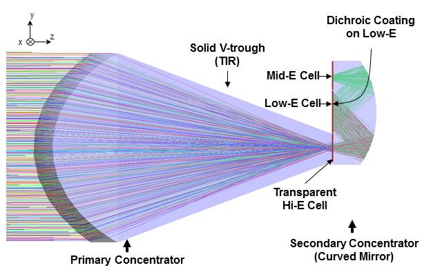 |
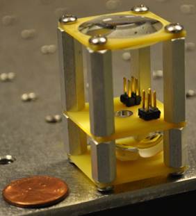 |
| (a) | (b) |
 |
|
| (c) |