ECE445 Tutorial 3 � Resistor,
Capacitor and MOSFET Layout
This tutorial will introduce you to the layout and extraction of resistor, capacitor and MOSFET layout in Cadence Virtuoso. The Cadence library for this tutorial can be downloaded by clicking here. Use gunzip to unzip the directory and add the library to your cds.lib .
Process Information and Design Rules
For the fabrication of chips in ECE 445, On Semiconductor 500 nm (C5 with two polysilicon layers
and 3 levels of metal) is used with a MOSIS technology code of SCN3ME_SUBM with
a lambda of 300 nm. MOSIS
information for this process is located here.
The C5 process data can be accessed
by clicking on of the process runs on this page. The C5
layout uses the MOSIS SUBM Design rules which can be accessed by
selecting the layers names on this page.
The NCSU Cadence Design Kit (CDK) technology file corresponding to the C5 process is called NCSU_Techlib_ami06 and should be visible in your library manager. When you create a new library, make sure you attach this techfile to the library.
LSW (Layer Selection Window)
The Layer Selection Window
(LSW) lets the user select different layers of the mask layout. Cadence
Virtuoso always uses the layer currently selected in the LSW for editing. The
LSW can also be used to restrict the type of layers that are visible or
selectable. To select a layer, simply click on the desired layer within the
LSW.
Note: Only layers with the dg property
are translated into the mask and will be fabricated. The rest of the layers
(net, label, pin, etc.) are used for labeling, highlighting errors, and for
text.
Following layers are
available in the NCSU CDK setup:
|
NCSU
CDK Layer Name |
Description |
GDS
layer number |
CIF
layer name |
|
nwell |
N-well |
42 |
CWN |
|
pwell |
P-well |
41 |
CWP |
|
active |
Active |
43 |
CAA |
|
nactive1 |
N-active |
43 |
CAA |
|
pactive1 |
P-active |
43 |
CAA |
|
nselect |
N-select (implant) |
45 |
CSN |
|
pselect |
P-select (implant) |
44 |
CSP |
|
Poly |
Polysilicon 1 |
46 |
CPG |
|
elec |
Polysilicon 2 (top electrode) |
56 |
CEL |
|
cc |
Generic contact |
25 |
CCC |
|
ca2 |
Metal1-active contact (obsolete, use cc instead) |
48 |
CCA |
|
cp2 |
Metal1-poly contact (obsolete, use cc instead) |
47 |
CCP |
|
metal1 |
Metal layer 1 |
49 |
CMF |
|
via |
Metal 1-metal 2 via |
50 |
CVA |
|
metal2 |
Metal layer 2 |
51 |
CMS |
|
via2 |
Metal 2-metal 3 via |
61 |
CVS |
|
metal3 |
Metal layer 3 |
62 |
CMT |
|
glass |
Overglass cut |
52 |
OCG |
|
pad |
Bon pad marker |
26 |
XP |
|
highres |
High resistance implant |
34 |
CHR |
|
sblock3 |
Silicide block |
29 |
CSB |
|
text |
Text layer |
|
|
|
res_id |
Resistor marker |
|
|
|
cap_id |
Capacitor marker |
|
|
|
dio_id |
Diode marker |
|
|
|
Nodrc |
DRC exclusion layer |
|
|
Note:
1 nactive and pactive are simply convenience layers for the user and not mask layers. They are treated as active for DRC, extraction and when the layout is streamed out. In the NCSU CDK cells, nactive is used for the active under nselect implant and similarly pactive layer is used for the active layer under the pselect implant.
2 These layers are obsolete, use the generic contact cc instead.
3 This layer is not available in the C5 0.5μm CMOS process. Use highres layer with poly2 to realize high value resistors.
Resistor Layout
Integrated resistors can
be made by different layers (active, well, poly). In analog applications linear
resistors are usually required, so that they are typically implemented using
poly, and if technology allows, using a special high resistive poly layer. The
procedure for designing a resistor is as follows:
a)
Determine the number of squares required by the resistor geometry (Num of
squares = Rreqd/R). Typical sheet resistances are
20-30 Ω/ for silicided poly and about 1 kΩ/ for the high-resistive
poly (See the link
for C5 process data). Note that the silicide block layer is not available in
the C5 CMOS process.
b)
Choose the width W
of the resistor
strip. It should be larger than the minimum given by the Design Rules for fabricating resistors.
c)
Obtain the length L
of the resistor
strip: L=
W x Num of Squares.
d)
If L is too long, several bends can be
introduced (thus forming serpentine resistors). Recalculate (b) counting about
0.6 square for each bend corner. You may also use unit cell
based resistor layout to avoid the bends and for better matching across
resistors.
Poly1
resistor
� Draw Poly
a) Select the poly layer from the LSW window.
b) Select the Create→Rectangle (or
choose the Rectangle icon from the side toolbar. The bindkey
for rectangle is r).
c) Draw a poly rectangle of width W and length slightly larger
than L (for allowing contacts at the resistor ends).
You may alternatively use the Path command with width W for
drawing longer resistors. The bindkey for rectangle
is p.
� Place Contacts
a) Select the contact layer (cc) from the LSW window.
b) Draw the contact rectangle on the extremes of the poly strip.
Note that the C5 design
rule requires the contact to be square of fixed size (2 X 2), or 0.6μm
X 0.6μm.
� Identify the device as a
resistor
If the Design Kit does not extract resistances by default (as for
the AMI technologies in the NCSU Kit) a layer called res_id
is provided to identify where a resistor is, and to obtain its resistance value
during netlist extraction. The res_id layer is not
fabricated.
a) Select the res_id layer from the LSW
window
b) Draw a rectangle of length L limited by the contacts and
surrounding the resistor.
� Metal Wires and Pins
a) Select the metal1 draw layer from the LSW window.
b) Place the metal over the contacts.�
c) Select Create→Pin to create
pins using metal1 layer at each end of the resistor. (The bindkey
for pin command is ctrl+p).

Figure 1 A poly resistor in C5
process.
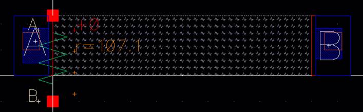
Figure 2 Extracted view of the poly
resistor.
High-Res
resistor
Some technologies offer a
highly resistive polysilicon layer, useful in analog design for obtaining
linear resistors of large values using small silicon area. In the C5 CMOS
process, they are made using the poly2 layer (elec in NCSU) and an
additional layer highres that defines the high-resistance region. The
procedure for creating high-res resistor in C5 CMOS technology is as follows:
� Draw Poly2
a) Select the elec layer from the LSW window.
b) Select the Create→Rectangle (or choose the Rectangle icon
from the side toolbar. The bindkey for rectangle is r).
c) Draw a poly2 rectangle of width W and length slightly larger
than L (for allowing contacts at the resistor ends).
You may alternatively use the Path command with width W for
drawing longer resistors. The bindkey for rectangle is p.
� Place Contacts
a) Select the contact layer (cc) from the LSW window.
b) Draw the contact rectangle on the extremes of the poly2 strip.
Note that the C5 design
rule requires the contact to be square of fixed size (2 X 2), or 0.6μm
X 0.6μm.
� Identify the device as a
high-res resistor
a)
Select the high_res layer from the LSW window
b)
Draw a rectangle of length L, separated from the contacts and surrounding the
resistor (according to the design
rules). Note that the design rules forbid placing the hi_res layer over the
contacts.
� Metal Wires and Pins
a) Select the metal1 draw layer from the LSW window.
b) Place the metal over the contacts.�
c) Select Create→Pin to create pins using metal1 layer at each
end of the resistor. (The bindkey for pin command is ctrl+p).

Figure 3 A hi-res resistor using �poly2 layer.

Figure 4 Extracted view of the hi-res
resistor.
Other
Resistors:
Resistors can also be made
using active or n-well layers, but the resulting resistances are strongly
nonlinear and temperature-dependent, and thus they are avoided in linear
circuit design. Their layout is very similar to that described for poly
resistors, substituting the poly layer by the proper layer. The res_id layer
should be present for extracting these resistances.
Capacitor Layout
In the C5 CMOS process, the
capacitors are made using two overlapping poly regions (poly1 and poly2) with a
thin oxide layer in between. The overlapping region defines the required
capacitance. Poly1 layer (poly in the LSW) is used for the bottom plate of the
capacitor and the poly layer (elec in the LSW) is used for constructing the top
electrode. The overlap of poly1 and poly2 defines the required.� The procedure for designing a poly-poly
capacitor is as follows:
a)
Determine
the poly1-poly2 overlap area for the capacitor geometry:
�Area = W�L = Creqd/Cox�
, where Cox� is the capacitance per unit
area. The poly1-poly2 overlap capacitance in C5 process is roughly 800-900 aF/μm2 (See the link for C5
process data).
� Draw elec
a) Select
the elec layer from the LSW window (this is the poly2 layer in NCSU
CDK).
b) Select
the Create→Rectangle (or choose the Rectangle icon from the side toolbar.
The bindkey for rectangle is r).
c) Draw a
rectangle with the area calculated previously.
� Draw poly
a) Select
the poly layer from the LSW window.
b) Draw a
rectangle overlapping the previous elec geometry according to the design
rules.
� Place Contacts
a) Use M1-poly
and M1-elec cells to create contacts from the NCSU library. You can use
the array option with sufficient spacing for creating multiple contacts at
once.
b) Place
the contacts on the top and bottom capacitor plates, fololwing
to the poly1
and poly2
design rules.
The
following figure shows a poly capacitor in the C5 0.5�m process.
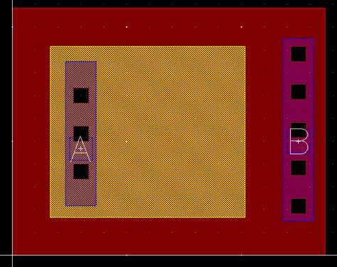
Figure 5 A poly-poly capacitor.
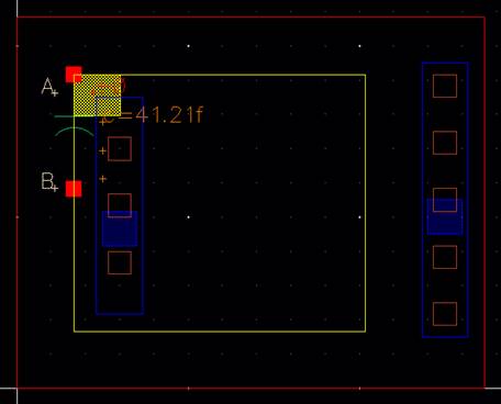
Figure 6 Extracted view of the poly-poly capacitor.
Note: The geometry of the capacitor need not be a square. In any case, if matched capacitors are required, they should not only have the same area but also the same geometry.
Contact
Layout Cells
Following readymade contact cells are available in the NCSU_Techlib_ami06 tech library for quick layout:
M1-P: Metal1-Pactive contact. This cell
is used for PMOS drain and source contacts, substrate contacts.
M1-N: Metal1-Nactive contact. This cell
is used for NMOS drain and source contacts.
NTAP: Metal1-Nwell Ohmic contact. This
cell is used in N-well contacts.
PTAP: Metal1-Substrate Ohmic contact.
This cell is used for the body contacts.
M1-POLY: Metal1-Poly contact. This cell is
used in transistor gate and poly resistor terminals.
M1-ELEC: M1 to poly2 contact. This cell is
used for the top plate contacts of poly-poly capacitors and in high-res
resistor terminals.
M1-M2: Metal1-Metal2 via.
M2-M3: Metal2-Metal3 via.
You may use the appropriate array options to place several contact or via cells. To create the contacts, Select Create→Via, then select the type of contacts and the number of contacts required in the pop-up window (shown below). For example, here we select a 4x4 array of NTAP contacts.
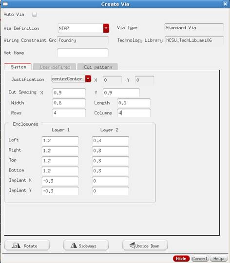
Figure 7 Specifying the contact cell array.
The resulting 4x4 NTAP array is shown below:
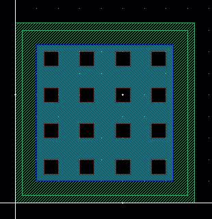
Figure 8 A 4X4 array of NTAP contact cells.
Custom MOSFET
Layout using Pcells
In MOSFET Layout we often use Multiplier and MultiFinger options to generate multiple instances of the same transistor, and hence to create an array of parallel and series connections respectively of a single transistor.
The parallel connected transistors are equivalent to a single transistor with effective width is Multiplier*Width and effective length is same as the length of any transistor. The Series connected transistors are equivalent to a single transistor with effective width is same as the Width of any transistors and effective length is Multiplier*length.
The library NCSU_TechLib_ami06 already contains pmos and nmos cells which can be used to generate the Multiplier and MultiFinger layouts.
Designing a PMOS transistor of
aspect ratio W/L
Select the Instance NCSU_TechLib_ami06 > pmos (Use Bindkey i for this purpose).
�The Create Instance window shown below:
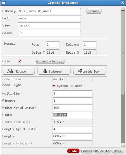
Figure 9 Create Instance for Pmos Multiplier
Multiplier option
Please enter the number of the transistors you want in parallel in Multiplier field along with the length and width of each transistor in the parallel connection. For example we want 5 transistors in parallel.
The create instance form looks like the following
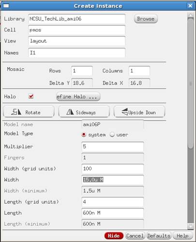
Figure 10 Multiplier value entered along with width and length
Note: Please observe that the Fingers option is grayed out as you enter Multiplier option. You could only use either of these options but not both of these.
So if Multiplier option is grayed out than enter a value of 1 in Fingers field, and hit cancel and press i once again so to enable the Multiplier option.
Now click Hide to place the five parallel transistors in your layout. The layout now looks like
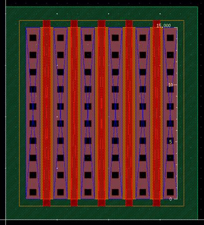
Figure 11 A PMOS with multiplier equal to 5
MultiFingers� option
Please enter the number of the transistors you want in series in Fingers field along with the length and width of each transistor in the parallel connection. For example we want 5 transistors in series. Enter the
The create instance form looks like the following
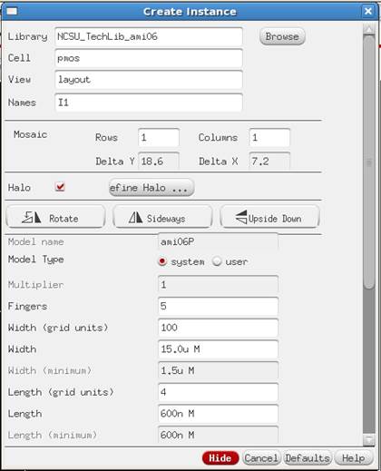
Figure 12 Creating PMOS using the Multi-Finger option
�����������������������������������������������
Now Click Hide to place the 5 series transistors in your layout. The layout now looks like the following:
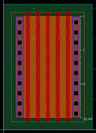
Figure 13 PMOS with five transistors connected in series
Note: Observe that the Multiplier option is grayed out as you enter Fingers option. So if Fingers option is grayed out than enter a value of 1 in Multiplier field, and hit cancel and press i once again so to enable the Fingers option.
Designing an NMOS transistor
Similar to the PMOS, just select the Instance NCSU_TechLib_ami06 > nmos and repeat the procedure as it was done for PMOS.
Long Length MOSFET Layout
An example layout for a long-length NMOS is shown below:
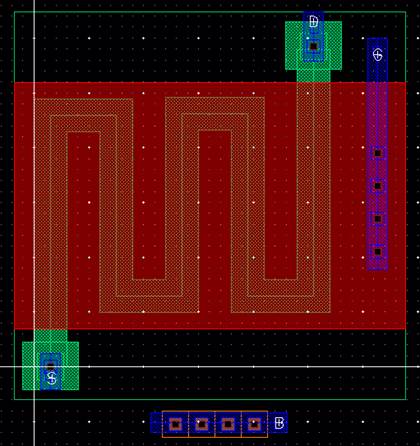
Figure 14 A long-length NMOS layout.
Here, the serpentine
nactive region is created using the Path (width = 3μm) command (bindkey is
p). Ntap cells are used for the drain and source contacts and Ptap cells
are used for the body contact. Also for the gate terminal, M1-POLY contacts are
used. You may like to explore the stretch (bindkey s) and merge commands
to help you lay out the serpentine structure.