ECE5410 Tutorial 1 – Schematic, layout and simulation of a
resistive voltage divider
Adapted
from CMOSedu Tutorial
1.
This
tutorial will introduce you to Cadence 6.1 for chip design, layout, and
simulation. To demonstrate the operation of Cadence we’ll set it up for
use
with On’s C5 process (formerly
AMI’s C5 process) and fabrication through MOSIS.
Schematic Design and Simulation
First, open a terminal window and follow directions shown below.
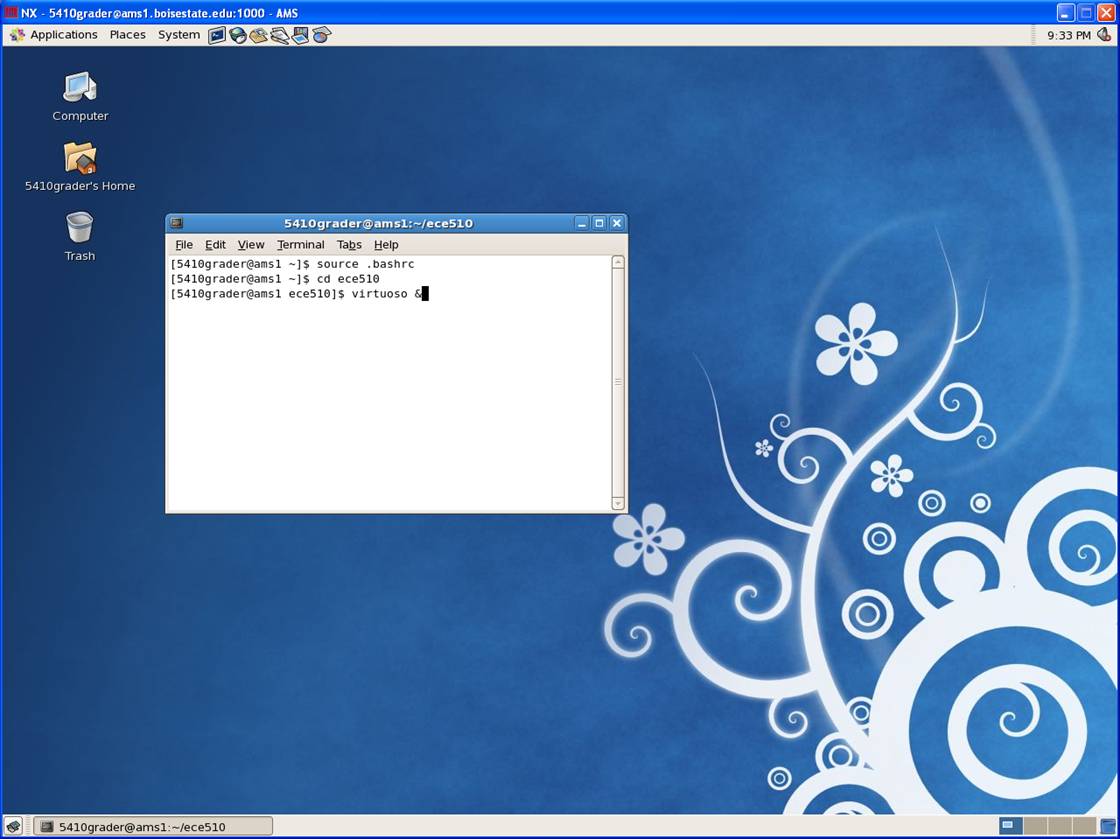
After starting Virtuoso, and re-sizing windows, the following should appear.
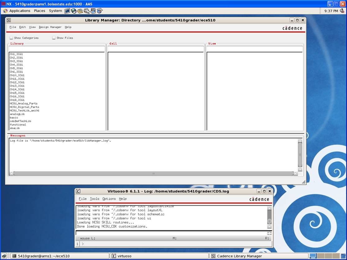
The bottom window is called the Command Interpreter Window or CIW. We need to keep the CIW visible since it tells us what the tools are doing. The
other window is the Library Manager. If this window isn’t open, or you close it, it can be opened in the CIW using Tools -> Library Manager.
Note, that the libraries for the relevant chapters for ECE510, from the CMOS textbook, are already loaded.
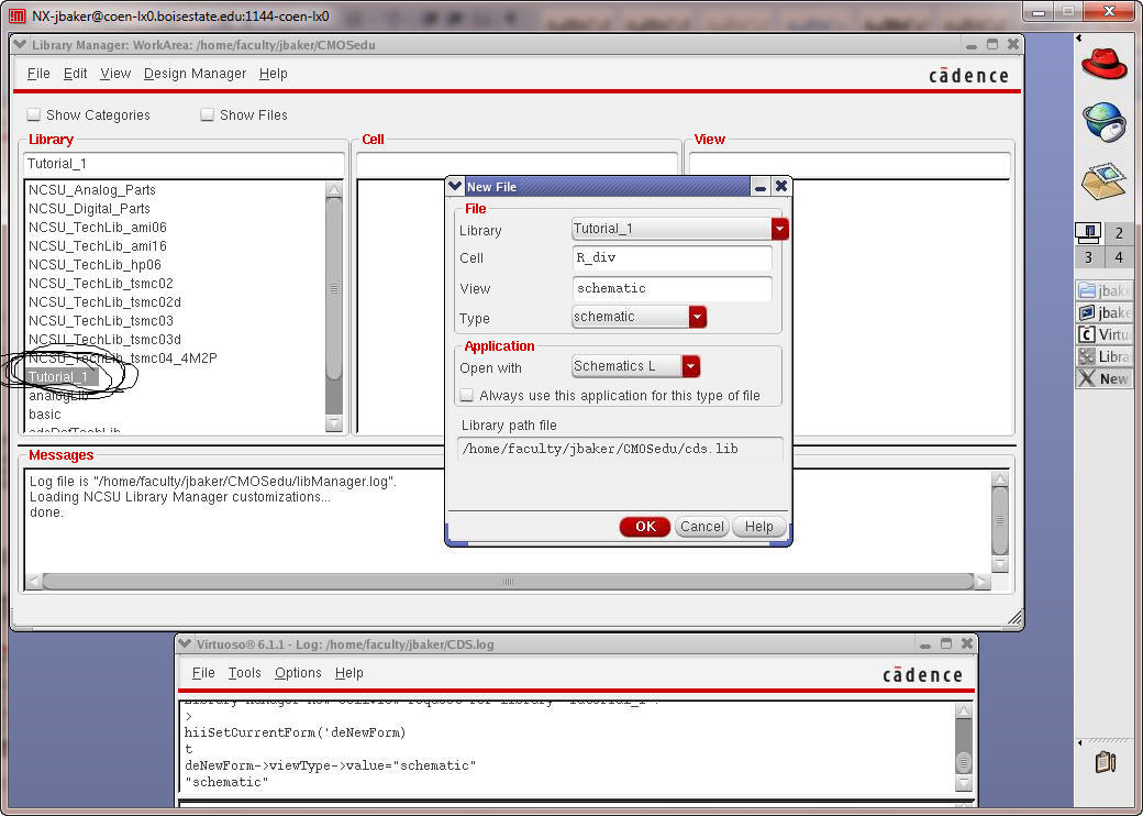
Next let’s create a new library by going to, in the Library Manager, File -> New -> Library. Call the library name as “Tutorial_1” and press “OK”.
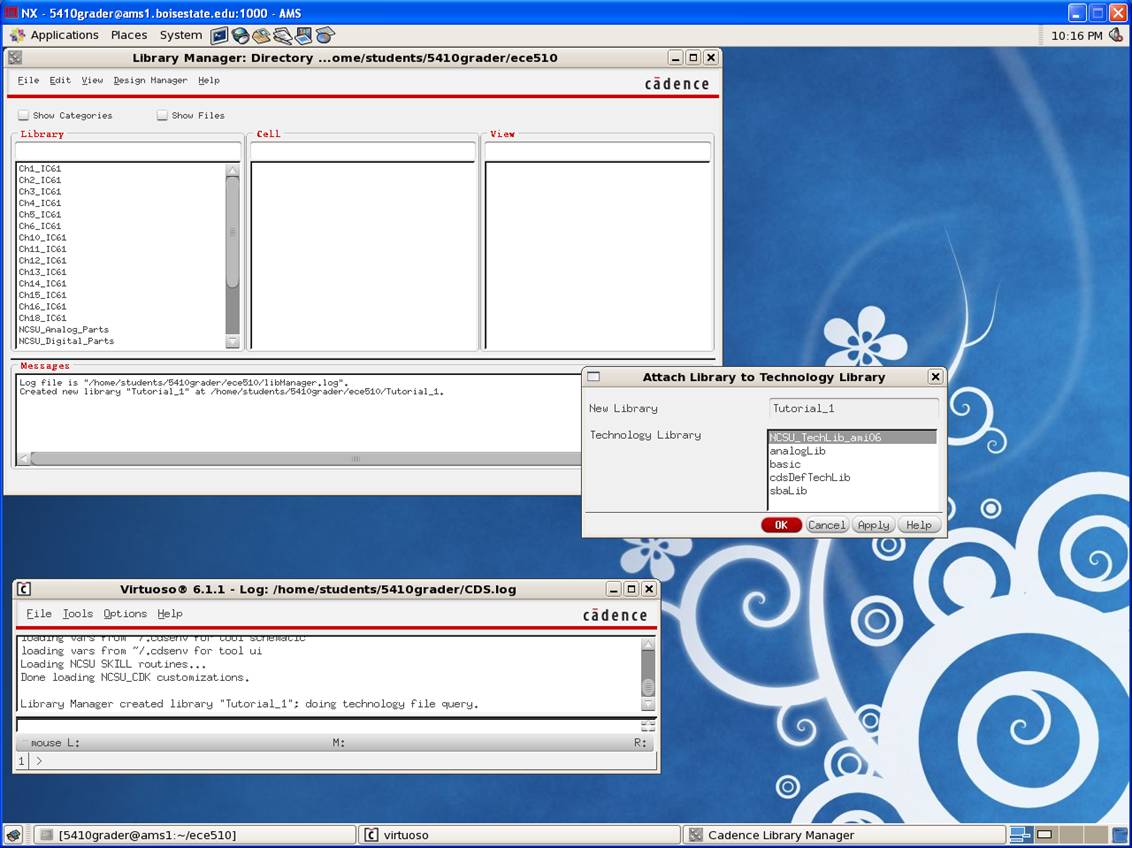
After pressing OK, another window pops up called “Technology file for New Library”. In this window, select “Attach to an existing technology library” and press OK.
It brings another window which shows the library name as “Tutorial_1” and technology library as “NCSU_TechLib_ami06”. Then press “OK”.
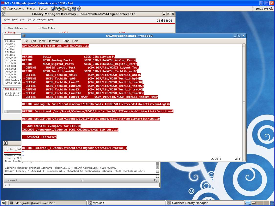
Let’s pause for a moment and look at the cds.lib file in the CMOSedu directory. As seen below when a library is created a definition line is added to the
cds.lib file.

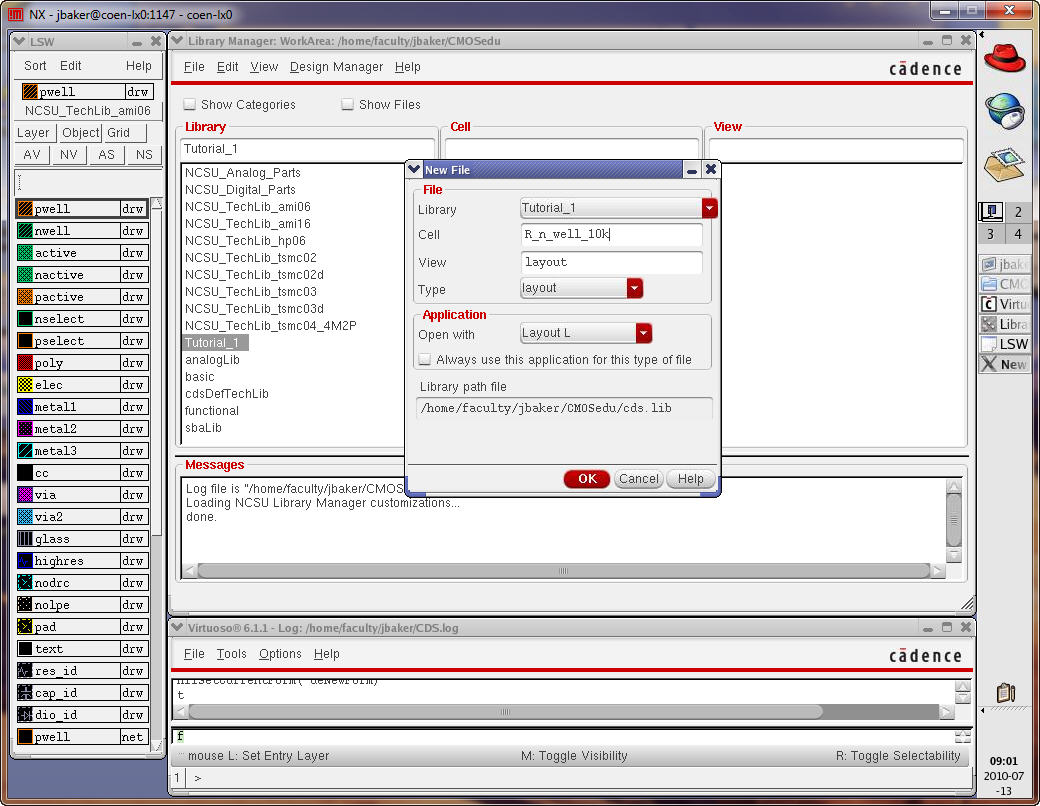
Next select the Tutorial_1 library in the Library Manager and then the menu items File -> New -> Cell View and enter the information seen below. Again
note that the window may be behind some other window.
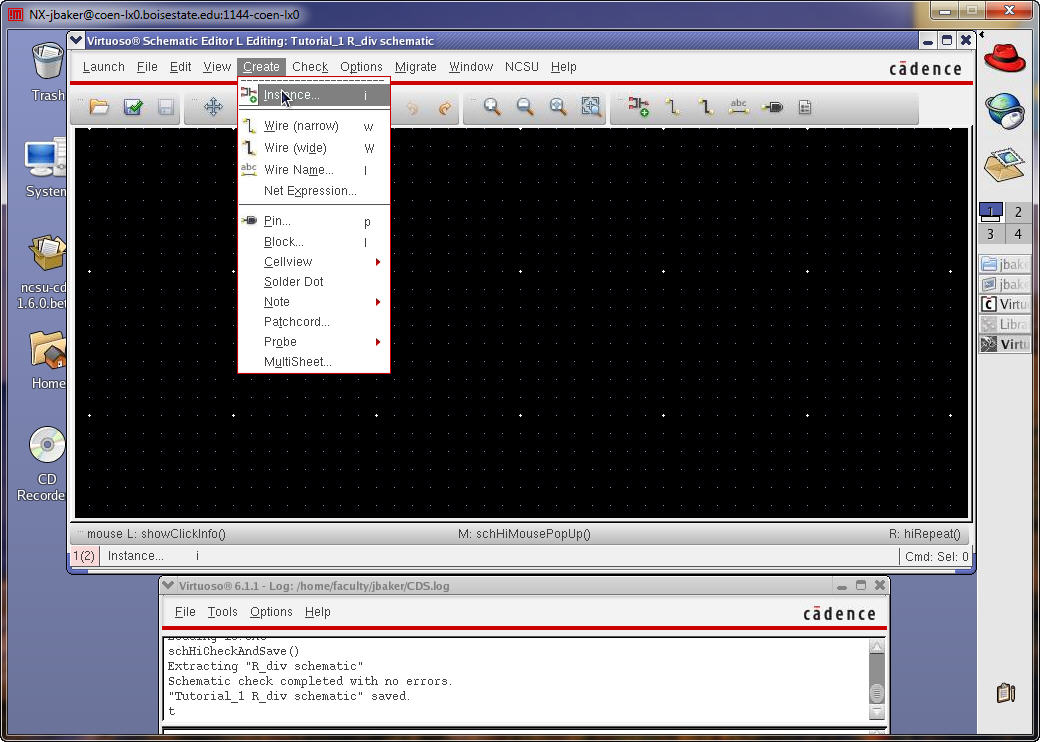
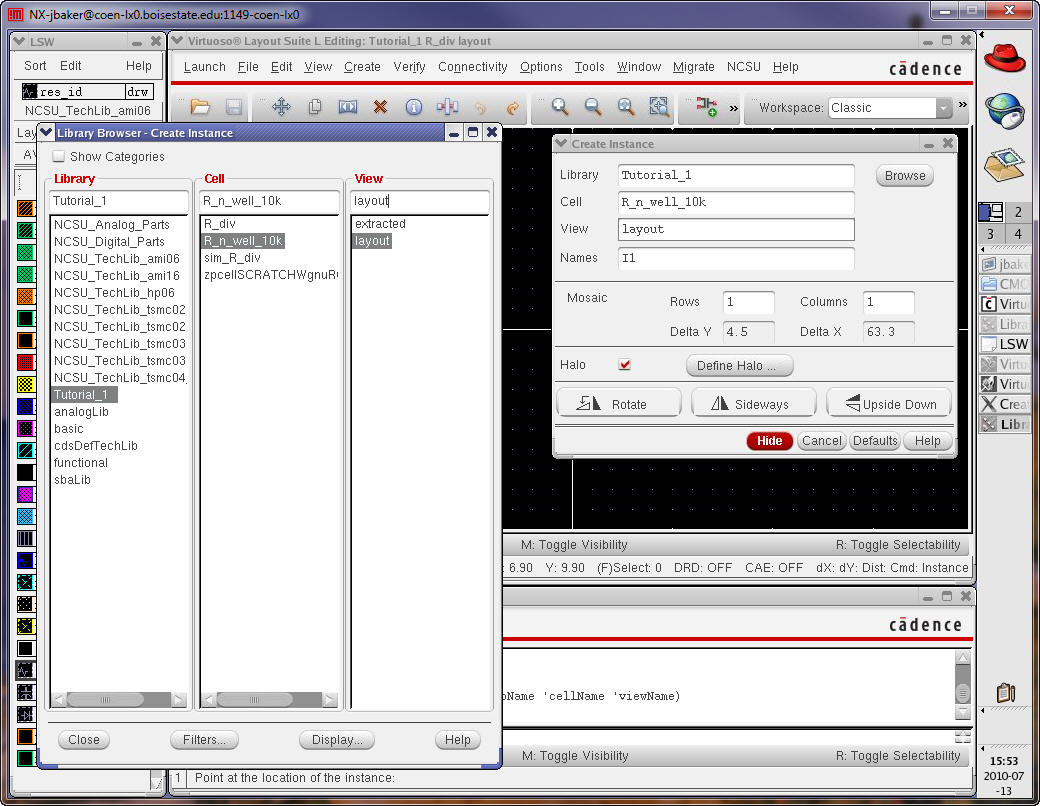
After selecting OK and resizing the window we can add a component (an instance) by going to Create -> Instance (or just pressing the Bindkey i or use the
menu item above the drawing display) as seen below.
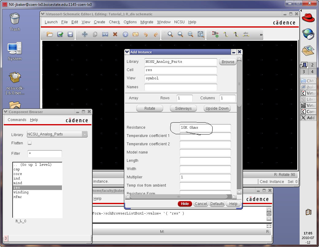
After re-sizing the window, selecting NCSU_Analog_Parts (in the Component Browser window), R_L_C, and res the following appears. Set the resistance
value to 10k as seen below.
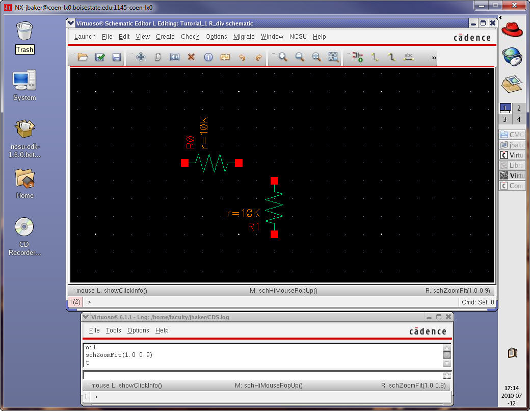
Hide the Add Instance window and minimize the Component Browser to the task bar. Add the two resistors as seen below. Right clicking the mouse button
rotates the symbol. Pressing Esc leaves the “Add Instance” mode.
Note that the Bindkey f fits the display. A listing of the Bindkeys is found here.
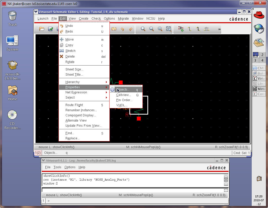
To change the resistor’s value select the resistor and use Edit -> Properties -> Objects (or just use the Bindkey q) as seen below. We’ll use this command often.
Click your mouse in the drawing area and press Esc a few times so that no commands are active.
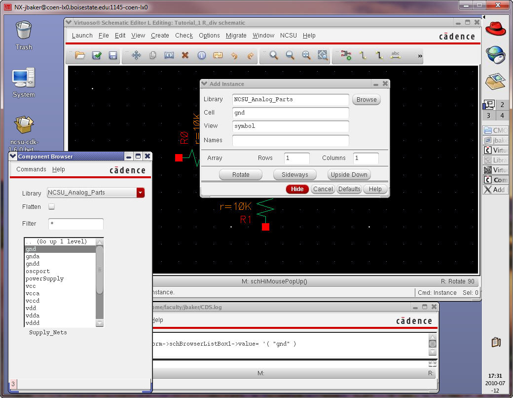
Next add ground to the schematic by pressing i (add instance) and maximizing the Component Browser, selecting Supply_Nets and gnd as seen below.
If you know the name and Library of the instance you want to add you can type them into the fields directly in the Add Instance window.
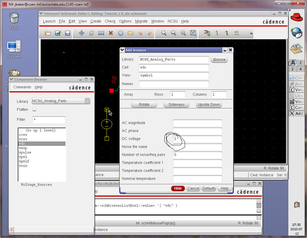
Add the ground symbol and then add a 1-V DC source, symbol name of vdc under Voltage_Sources as seen below.
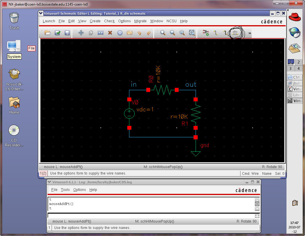
After placing the symbol we need to wire the circuit together. This can be done by using the Bindkey w (for wire) or the menu item as seen below.
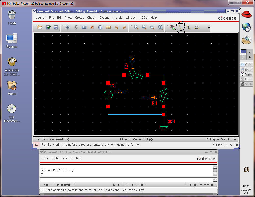
It’s often useful to label wires with signal names. Using the Bindkey l (lowercase L) or the menu item enables naming wires. Let’s do this as seen below.
We are about ready to simulate the operation of this circuit. Let’s do a “Check and Save” first. If we have edited the schematic and try to simulate
without checking and saving first the simulation will fail.

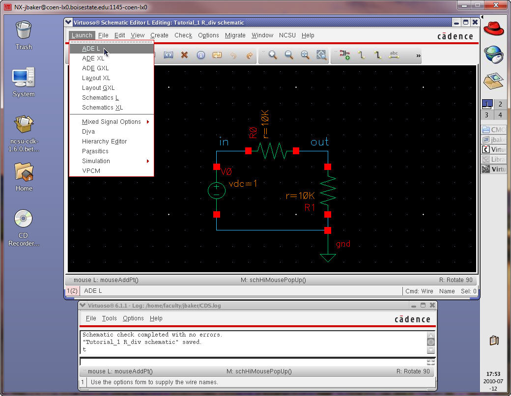
To simulate with Spectre (Cadence’s SPICE simulator) go to the menu Launch -> ADE L as seen below.
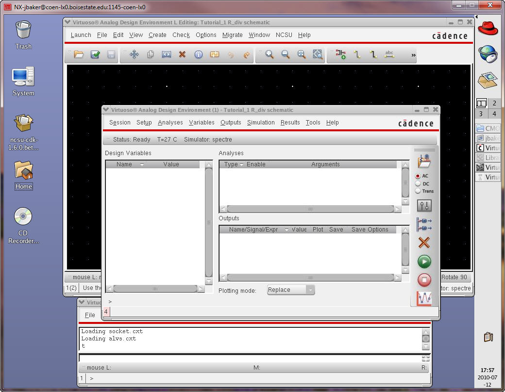
The Virtuoso Analog Design Environment (ADE) window should appear as seen below.
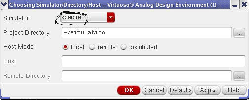
Use the menu in the ADE and go to Setup -> Simulator/Directory/Host to verify the simulator is set to spectre.
We’ll assume throughout these tutorials that spectre is used. If it’s not the default then please re-visit above instructions.
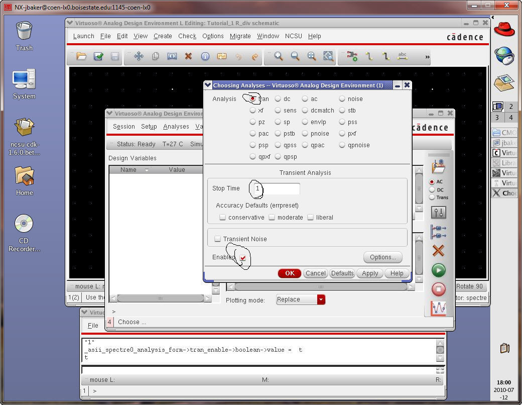
Next go to Analyses -> Choose and select a transient analysis (tran), a stop time of 1 second, and Enabled as seen below.
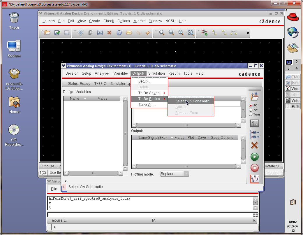
Next we need to select the signals we want to plot. Follow the menu items seen below selecting “Select On Schematic”.
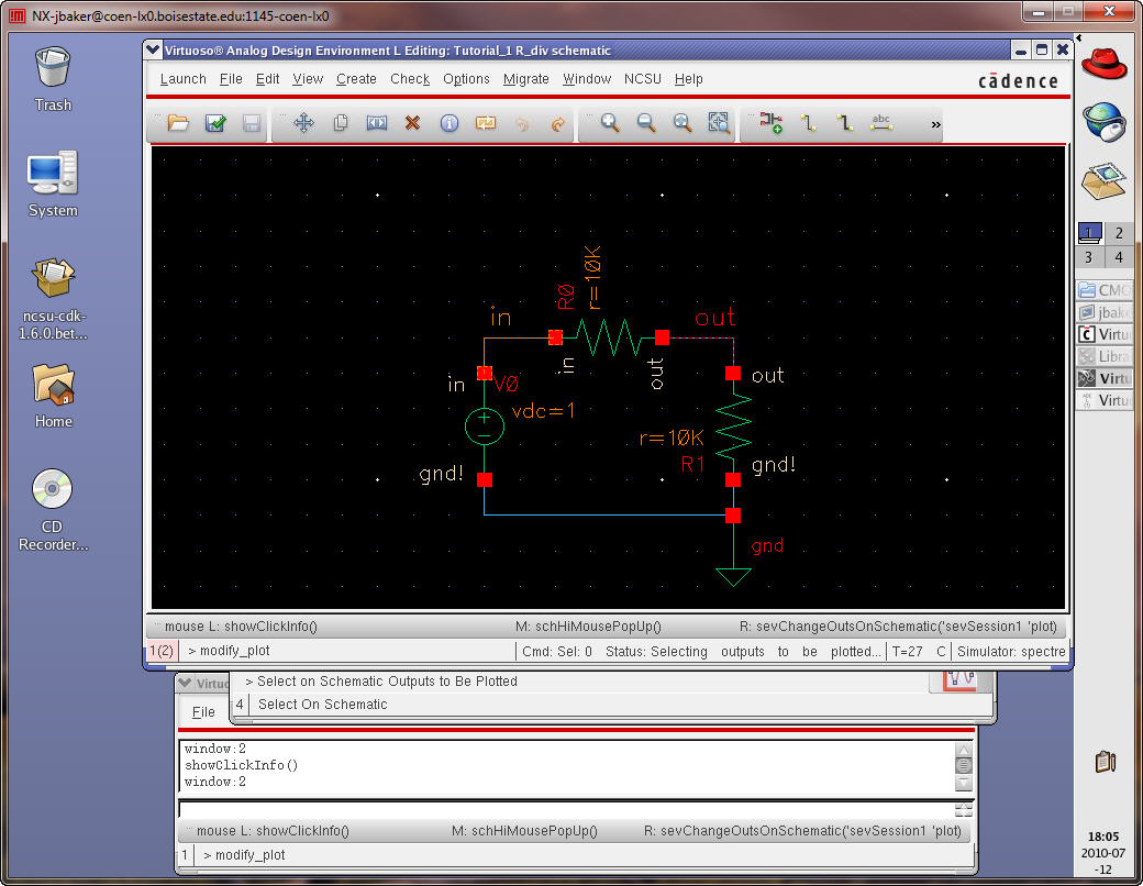
Select the wires as seen below.
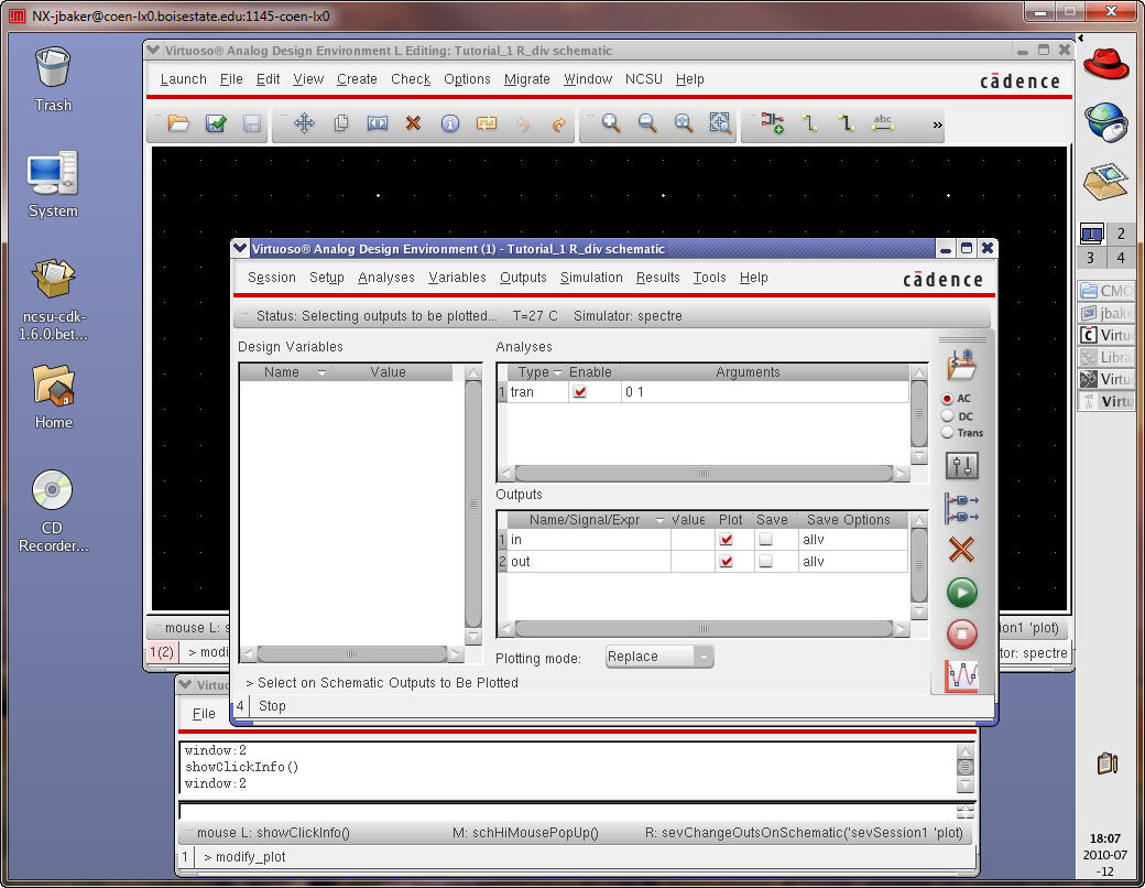
The ADE should now look like the following (bring the window to the front via the task bar).
We can now simulate the schematic by pressing the green “Netlist and Run” button. However, before we do this let’s save this information so that next time
we want to simulate this circuit we don’t have to go through these steps again.
In the ADE window use the menu
items Session ->
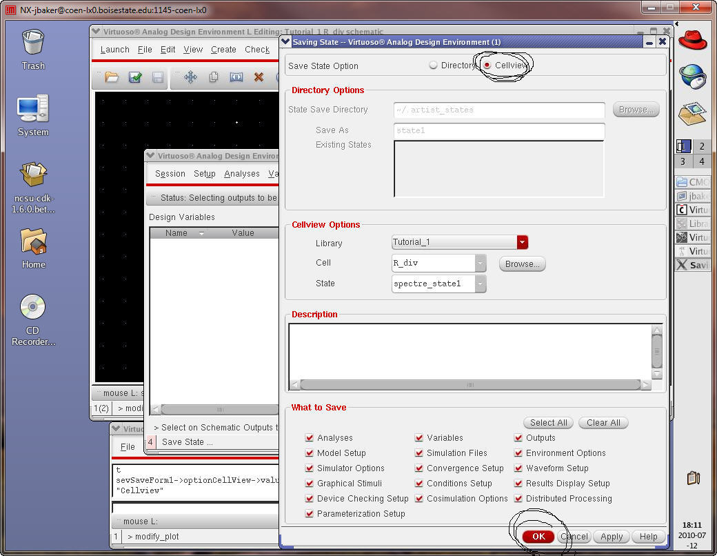
To load this state we select, in
the ADE window, Session ->
from CMOSedu.com.
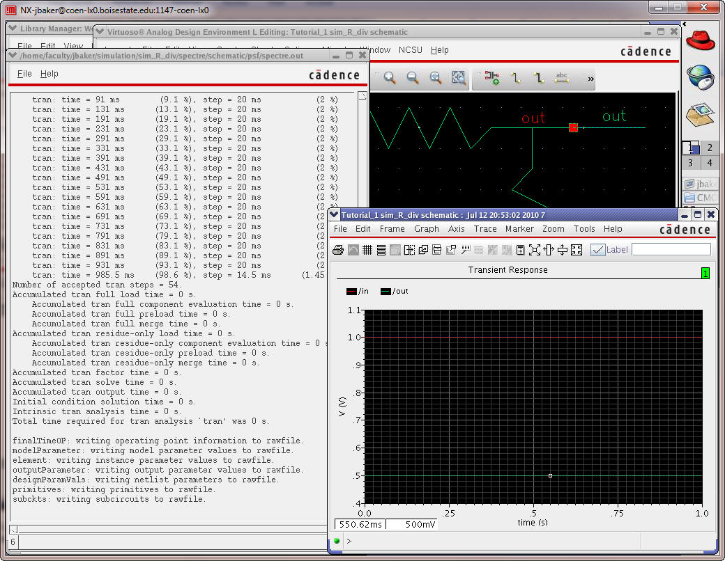
Now pressing the green button and running the simulation results in the following.
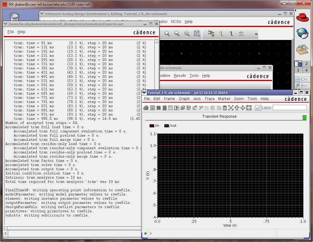
Which is, hopefully, what the reader expected ;-)
Let’s close the ADE and go back to the schematic.
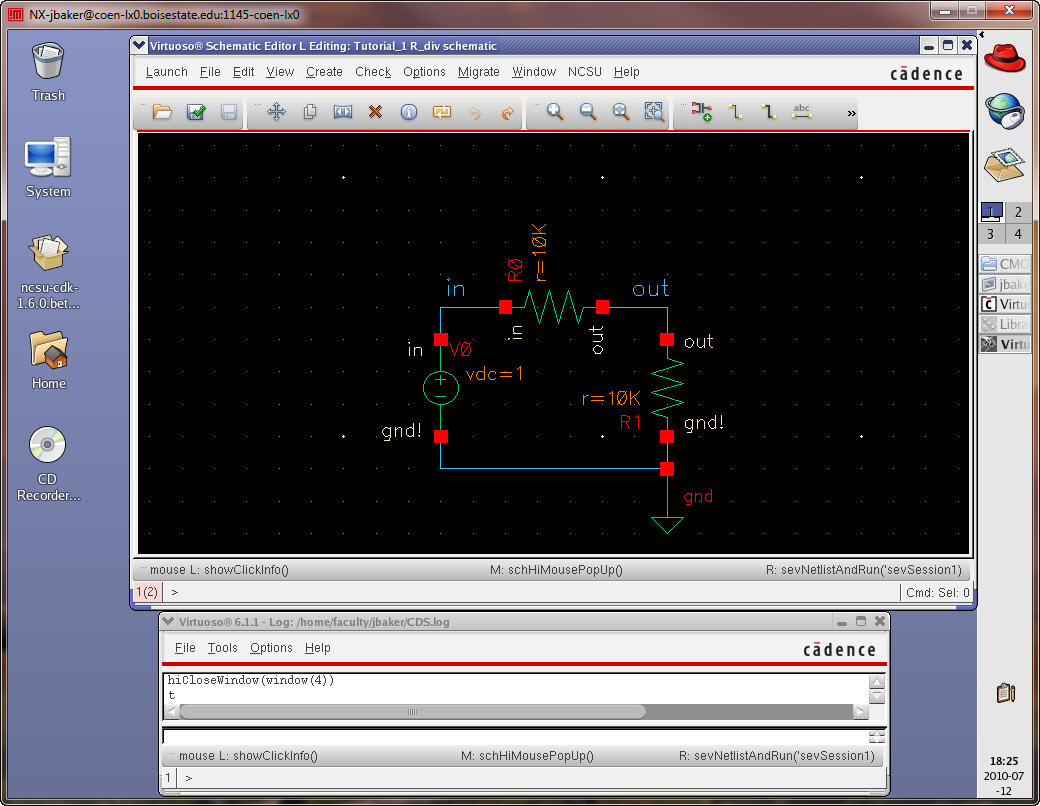
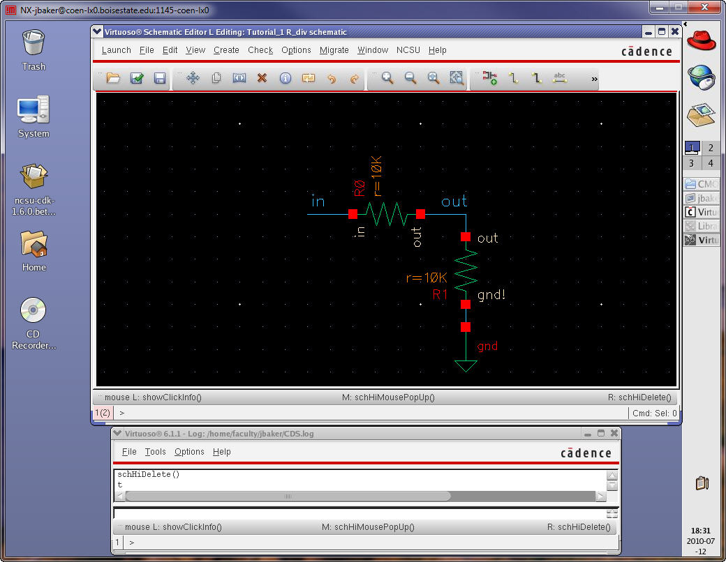
While this is a general purpose schematic let’s make it more useful as a cell in an integrated circuit. Select, and delete, the bottom wire and voltage source.
Note that once you select and delete one wire or component Virtuoso is in the delete mode so all you have to do is click on the next item you want to delete.
To exit this mode press Esc. To undo an action press u.
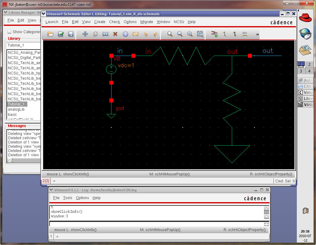
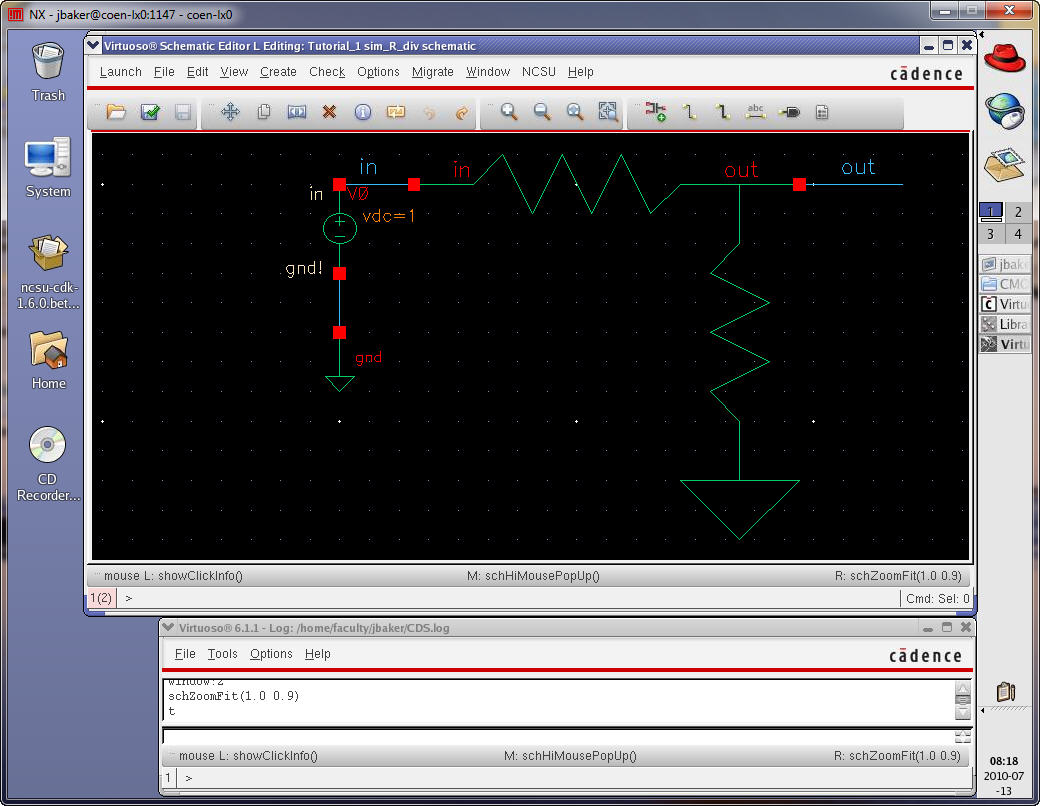
Ensure you have the following schematic.
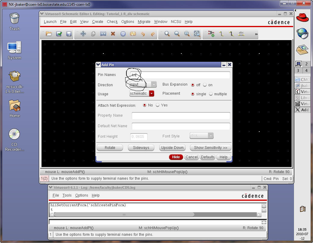
Let’s add pins to the schematic using the menu Create -> Pin (or the Bindkey p). Pins are what is used to connect the schematic symbol, which will make shortly,
up in a higher-ranking schematic view. Add an input pin called in (so it matches the wire name, useful but not necessary).
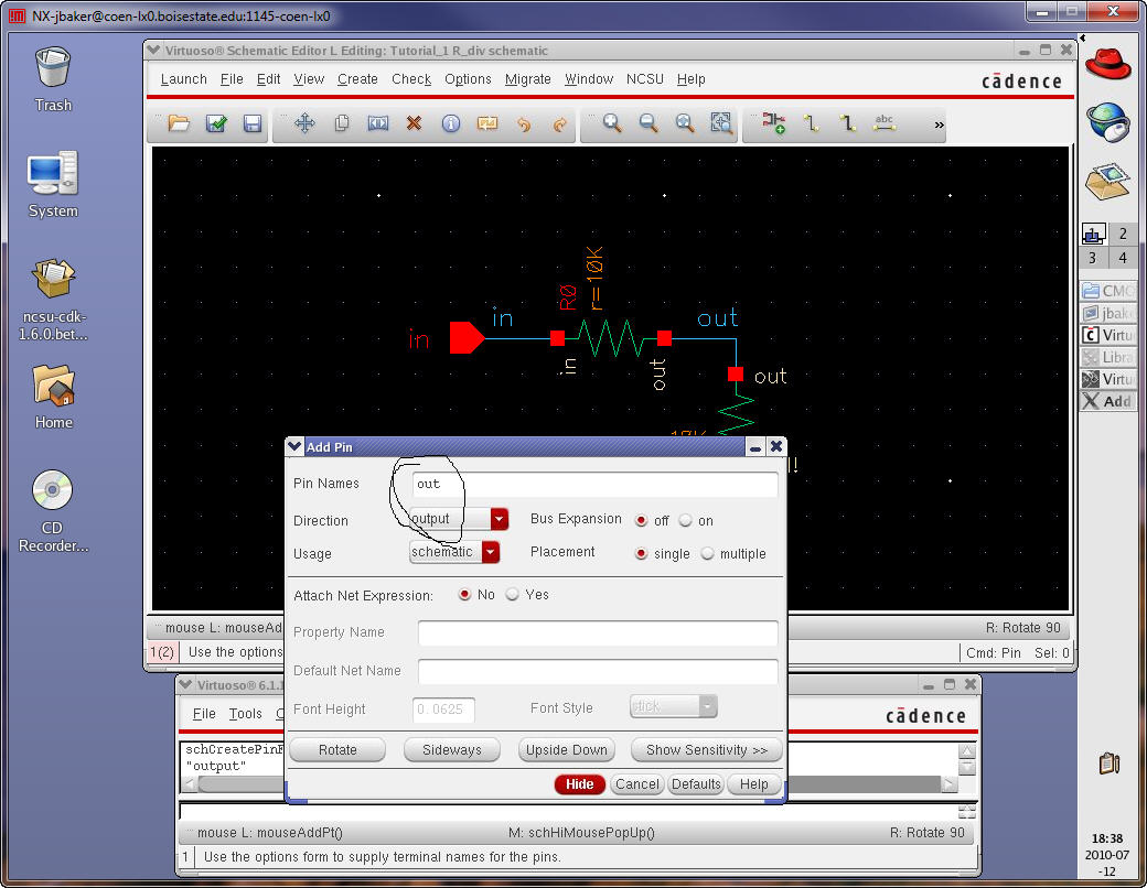
And an output pin.
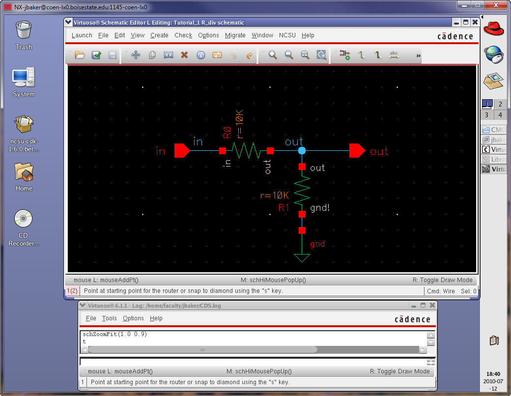
Adding a wire to the pin and “Checking and Saving” results in the following.
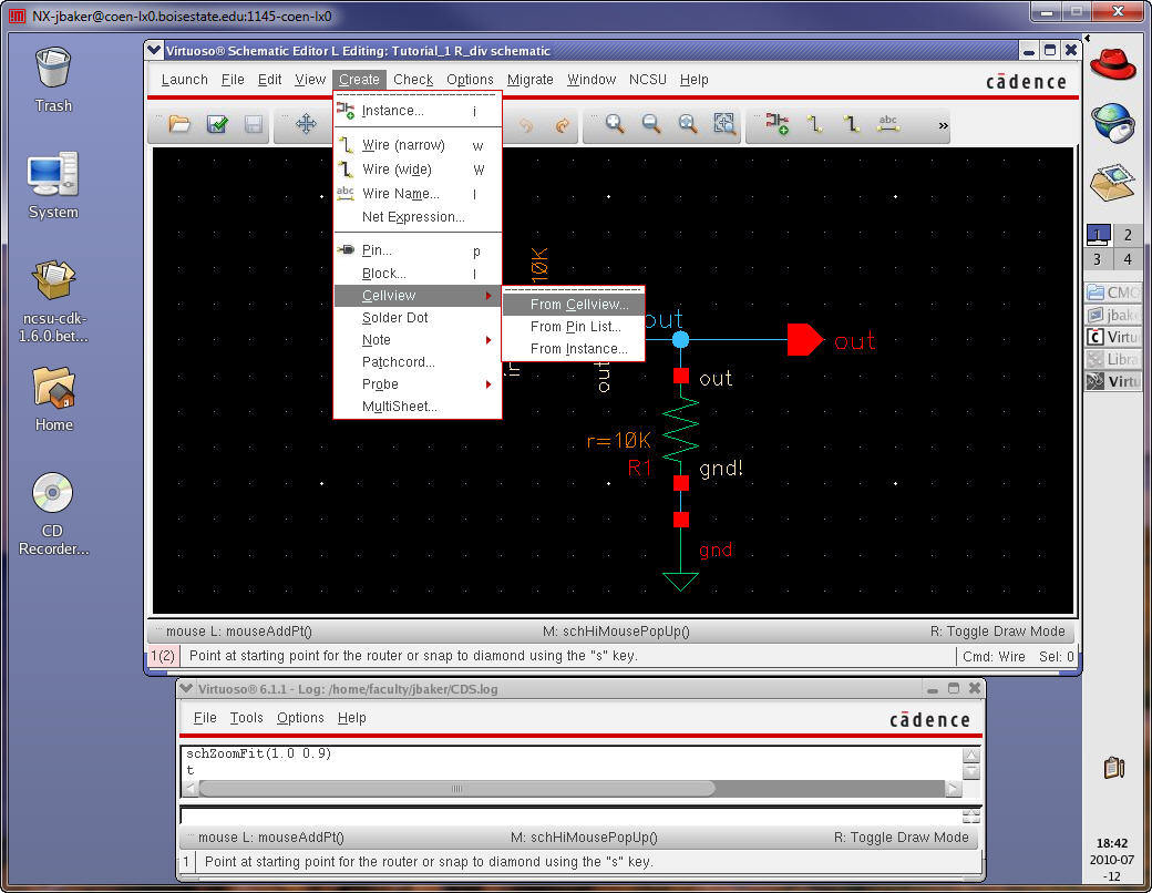
Let’s create a symbol for this schematic following the steps seen below.
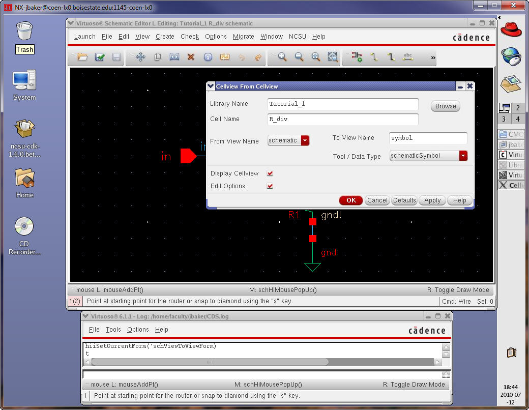
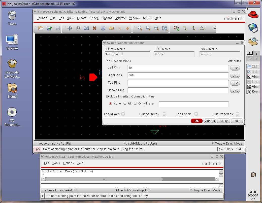
And finally,
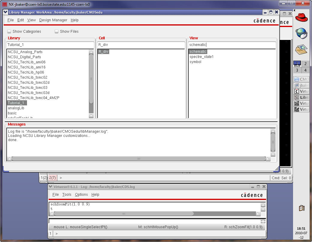
If we look at the Library Manager we see three Cell Views for the R_div group remembering that the spectre_state1 Cell View contains our simulation parameters
which we load when the ADE is started as mentioned above.
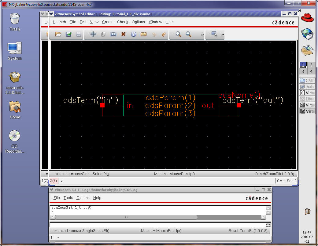
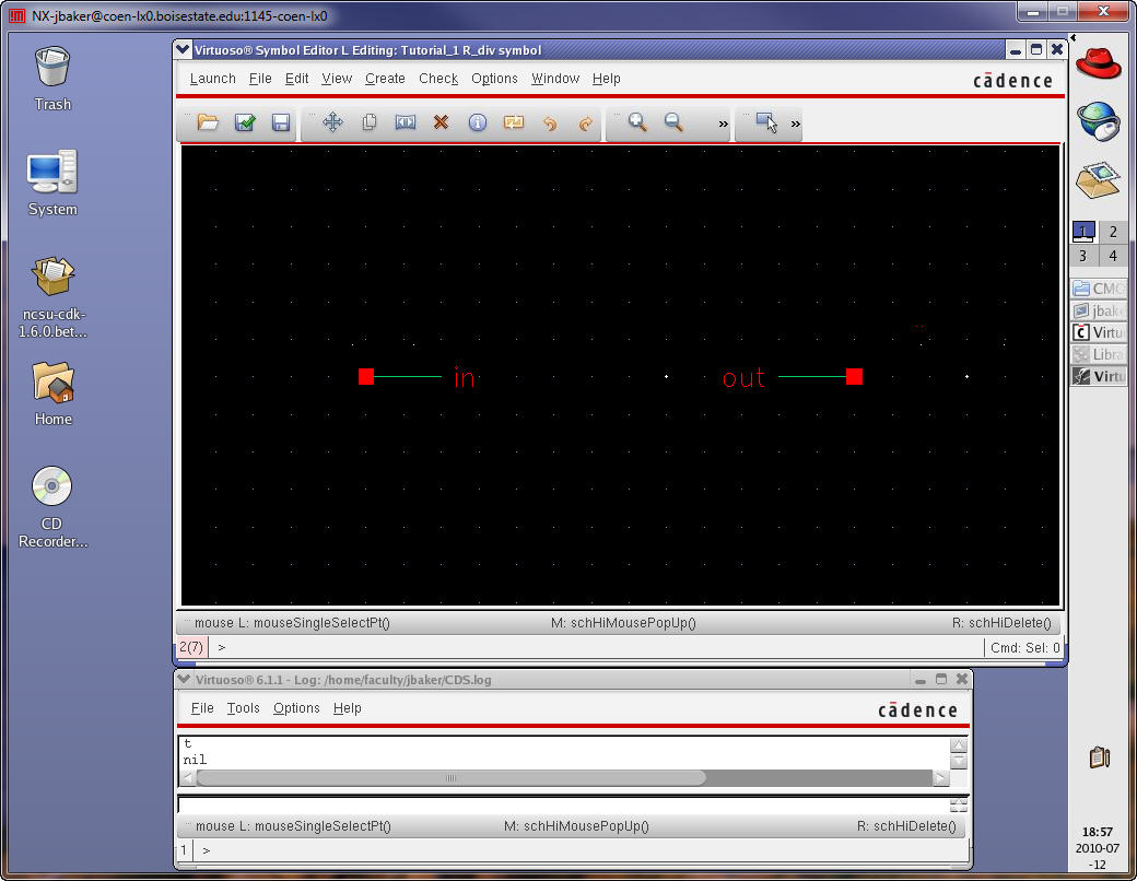
Let’s delete everything in the symbol view except for the following. Remember that you can always use the undo command (u) if you accidentally delete something.
Move the text and then add a line.
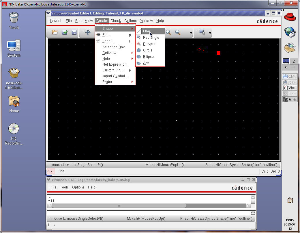
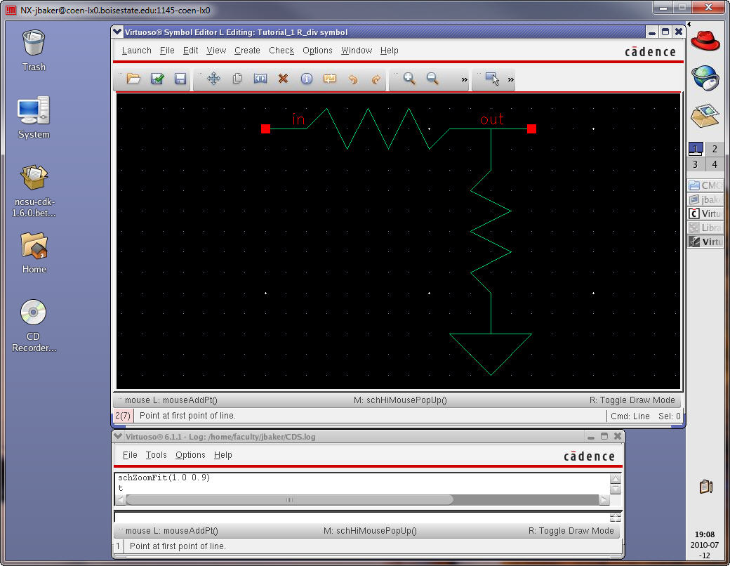
Draw the symbol seen below. Note that Z (zoom out by 2) and f (fit) can be useful when drawing the symbol.
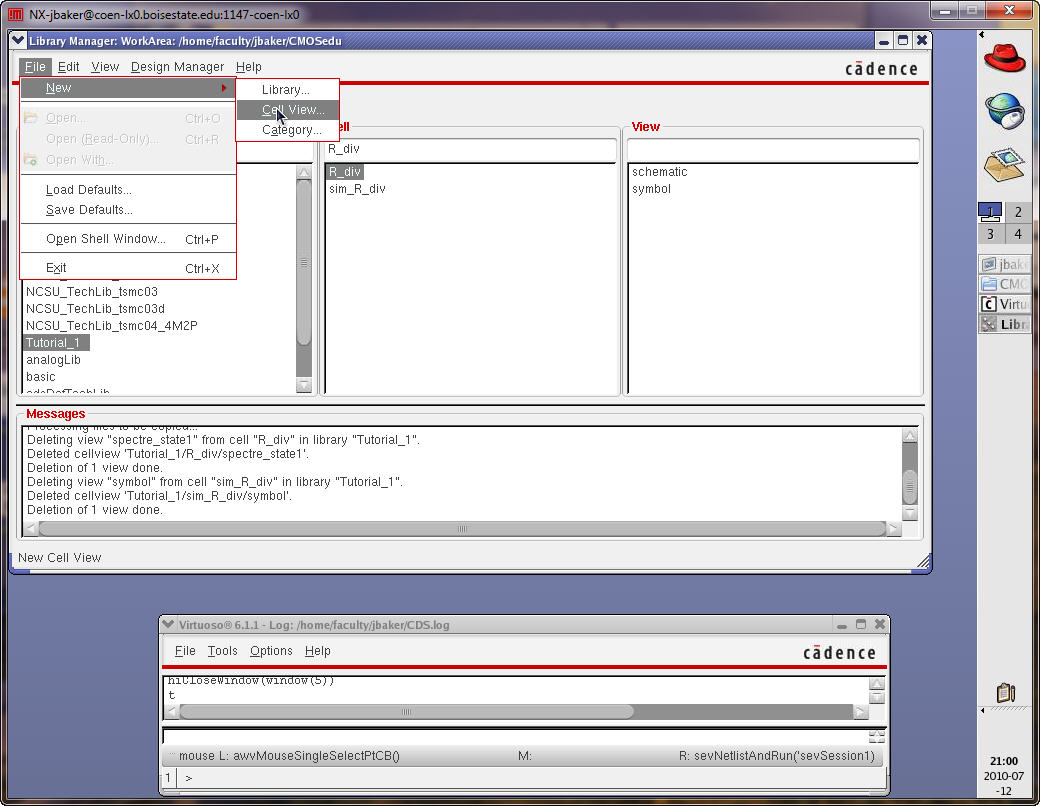
When finished Check and Save the symbol view. Close both the symbol and schematic views of the R_div cell. Before doing the layout for the R_div cell let’s
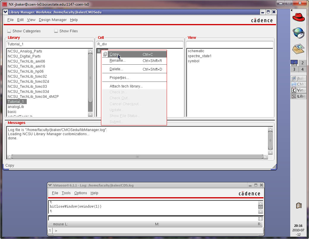
simulate the cell’s operation again. To speed things up copy R_div into another cell called sim_R_div (right click on the cell name).
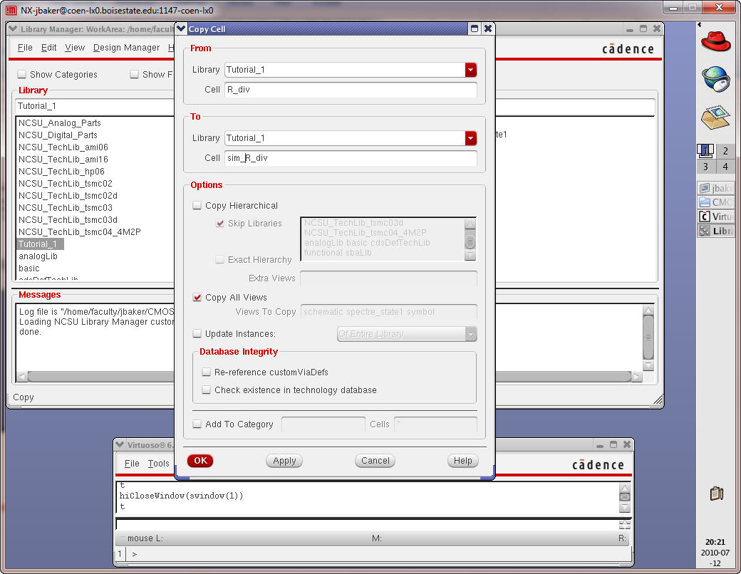
After hitting OK delete the spectre_saved1 in the R_div cell by right clicking on the name in the View category.
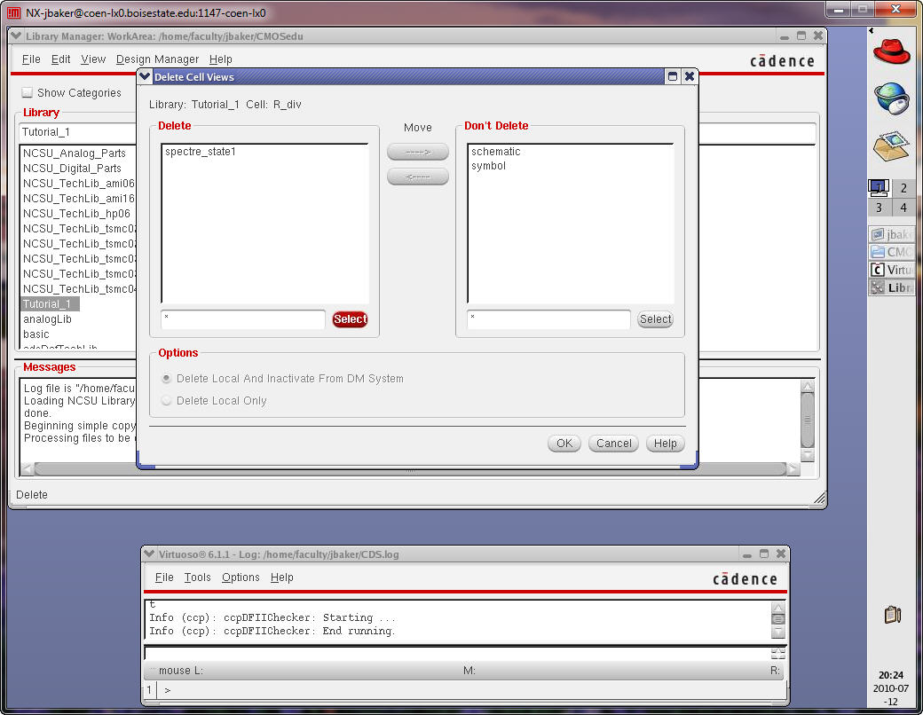
After hitting OK and Yes you are sure delete the symbol view in the sim_R_div cell.
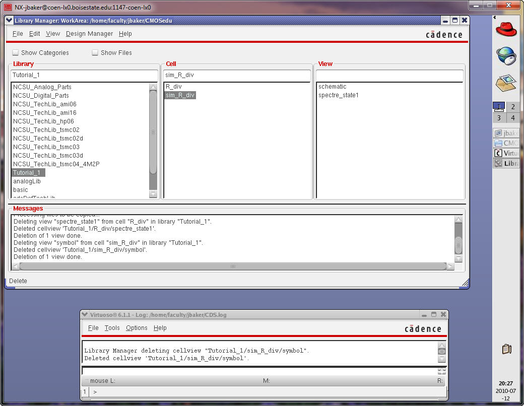
Next open the schematic view of the sim_R_div cell and delete everything in the cell.
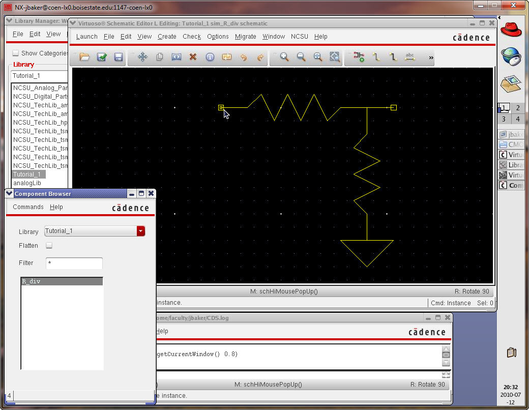
Press i to add the symbol for R_div in the Tutorial_1 library.
After you place the cell hit Esc to leave the place instance command mode.
Next add wires, wire names, and the input voltage like we did above.
Set the input voltage to 1 V DC.
When finished Check and Save the schematic.
Note we get two warnings.
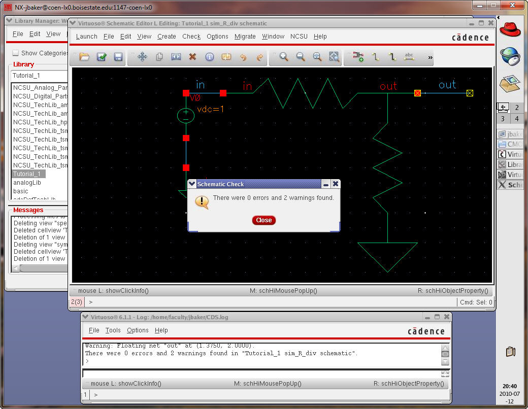
The warnings are from the floating wire named out.
Go to the menu items Check -> Find Marker to see the details.
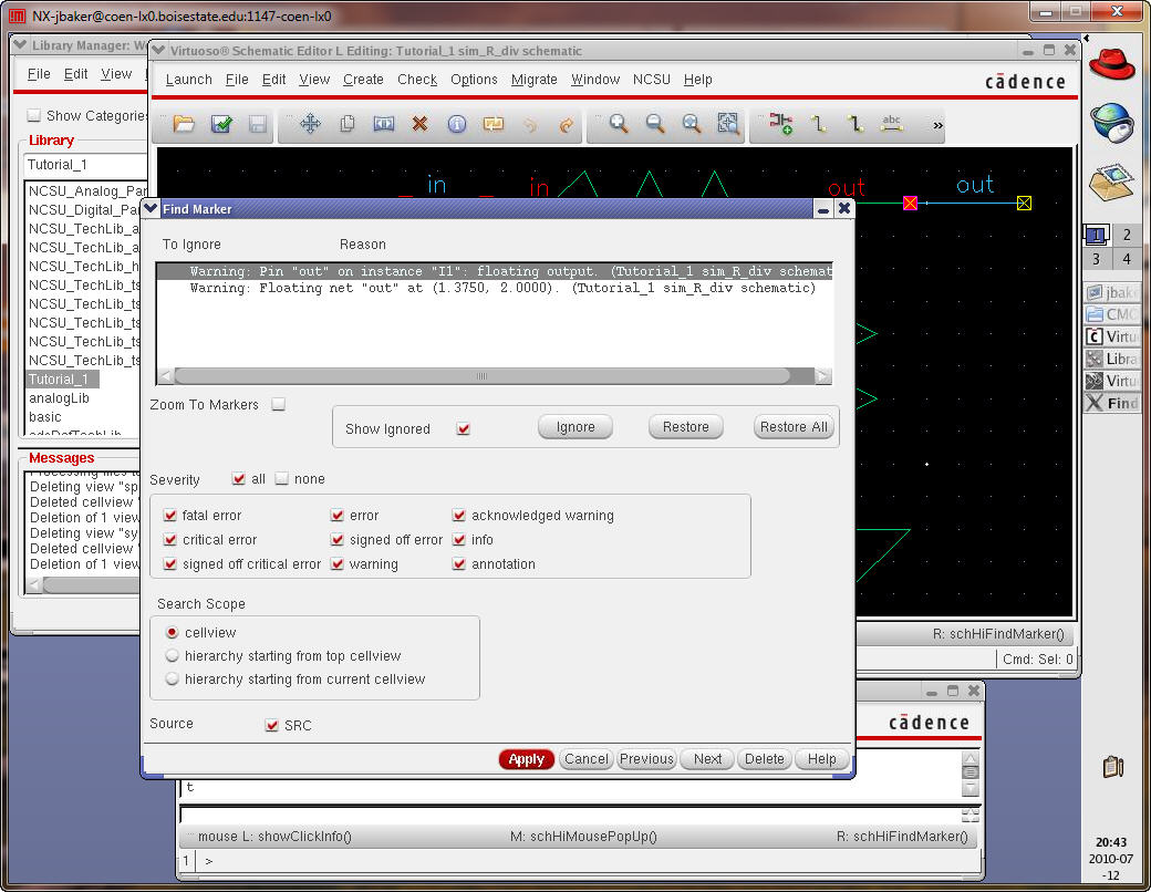
We are okay with this wire floating so press ignore twice and then close the Find Marker window.
Check and Save the schematic again. There should be no warnings or errors.
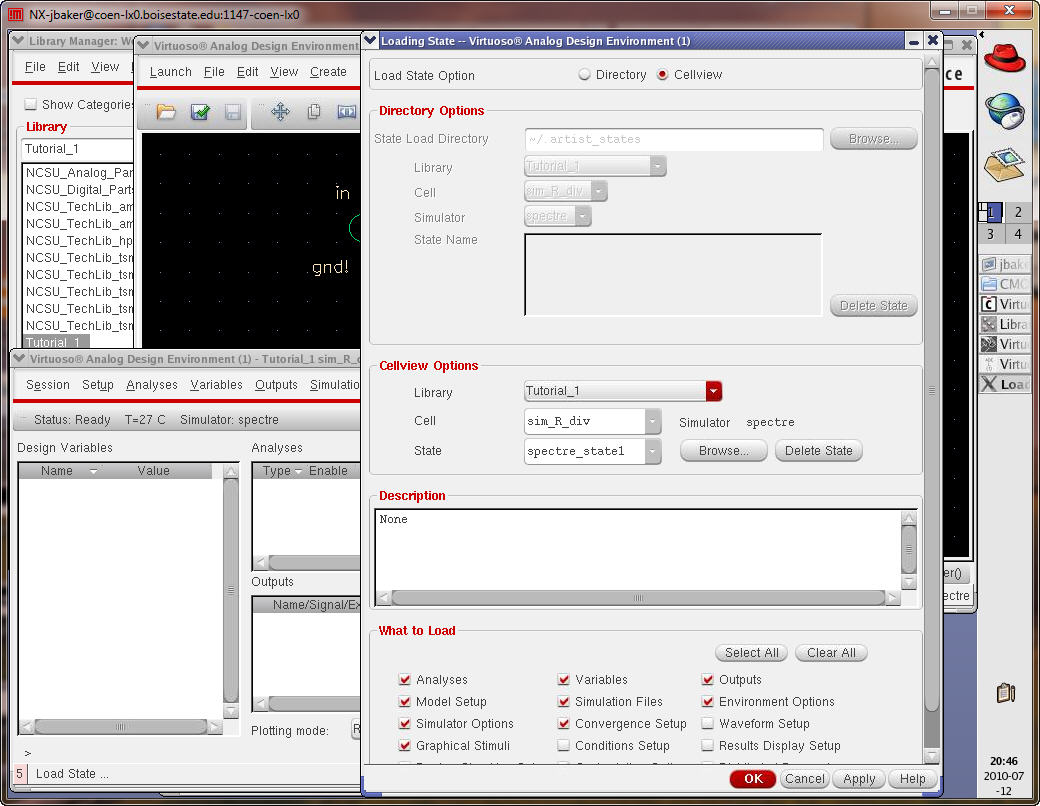
Now let’s simulate this circuit. Launch the ADE and then load the state (Cellview…important).
While the type of analyses will be remembered the outputs to be plotted won’t be remembered. Use the menu items Outputs -> To Be Plotted -> Select on Schematic
to select the in and out wire
nodes. Next use the menu items Session ->
the Spectre simulation.
Close the ADE.
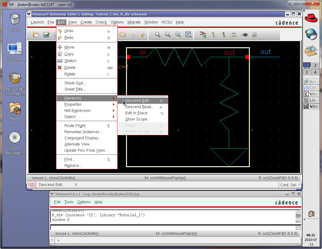
Before moving on to the layout lets cover one last item, that is, descending through the hierarchy.
Select the R_div symbol (left+click the mouse button on the symbol) and follow the menu items seen below (or just press X).
The contents of the symbol can be edited in the current tab (window) or in a new window. Select current tab and press OK.
Note, also, that you can return back up in the hierarchy by pressing b or the menu item seen below (but shaded since we are already at the top).
Descend down into the R_div schematic and then back up to the sim_R_div schematic to get some experience with the commands.
Layout
We are now ready to lay out the resistive divider.
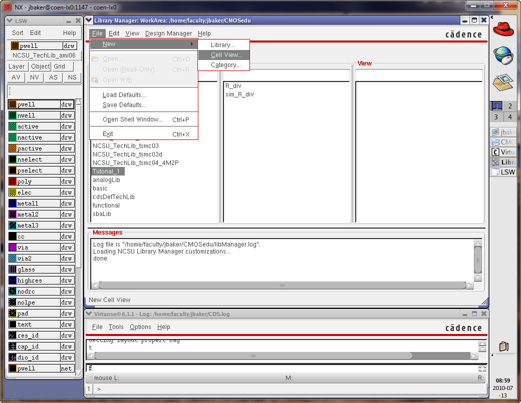
To begin make a new Cell View for the layout of R_div.
After creating the layout cell view the following will appear.
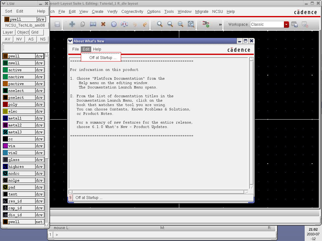
Select Off at Startup to ensure you don’t see this What’s New information each time you start-up a layout session.
Note the Layout Selection Window (LSW) that allows you to select specific layers when doing layout.
In the top of the LSW you can select AV (all layers visible) or NV (only the layer selected is visible). After making this selection follow it by re-drawing
the layout window (View -> Redraw) to see the results. AS and NS are used in a similar manner to allow selecting or not selecting specific layers.
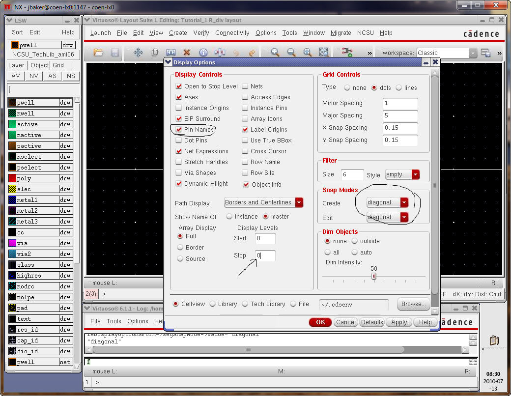
Next go to the menu items Options -> Display (or just press e).
Set the display so that Pin Names are shown.
Change the Snap Modes to diagonal .
Note that the Display Levels has no depth, that is, the layout of a cell placed in another cell will show as an outline. To see the contents we need to increase
the Stop level. We’ll do this later just so we can see this window again and what an outline of a cell looks like.
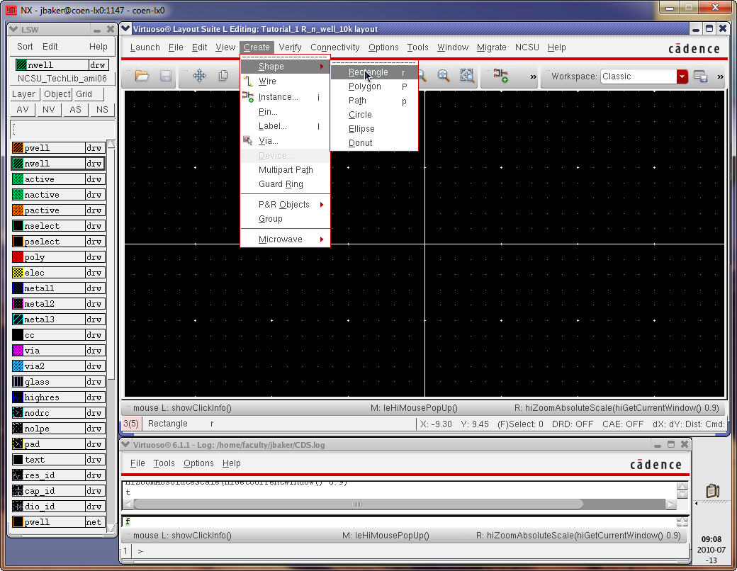
We are now ready to draw some shapes.
When we started drawing the schematic for the R_div cell the first thing we did was press i and place the symbol for a resistor. Here we don’t have a layout for
the resistor so we need to create one!
We’ll use the n-well layer for the 10k resistor.
The sheet resistance of n-well in
the C5 process is roughly 800 ohms.
The minimum width of n-well is 12 lambda (3.6 microns since lambda here is 300 nm) so let’s make a 10k resistor using a width of 4.5 um and a length 56 um.
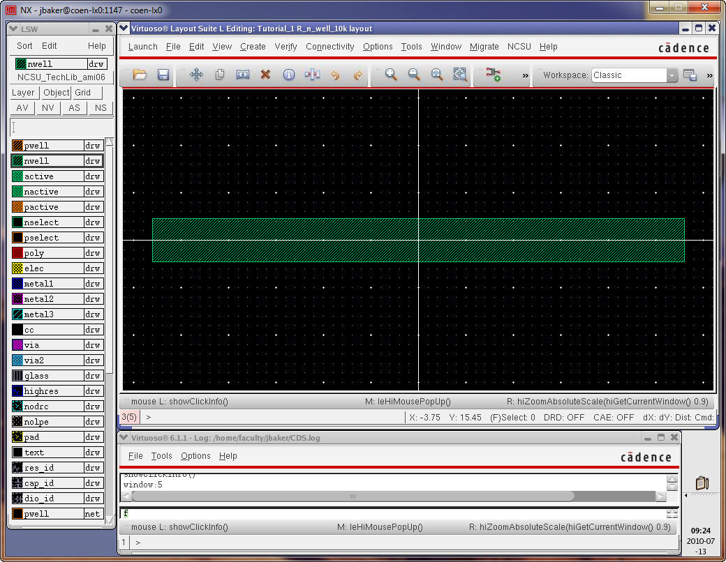
Create a cell (layout view) called R_n_well_10k.
Select n-well in the Layer Selection Window (LSW).
Next create a rectangle (this will be the resistor with a width of 4.5 um and a length of 56 um).
At this point don’t worry about the size. Click once to start drawing the rectangle then, after moving the mouse, click again to finish the drawing.
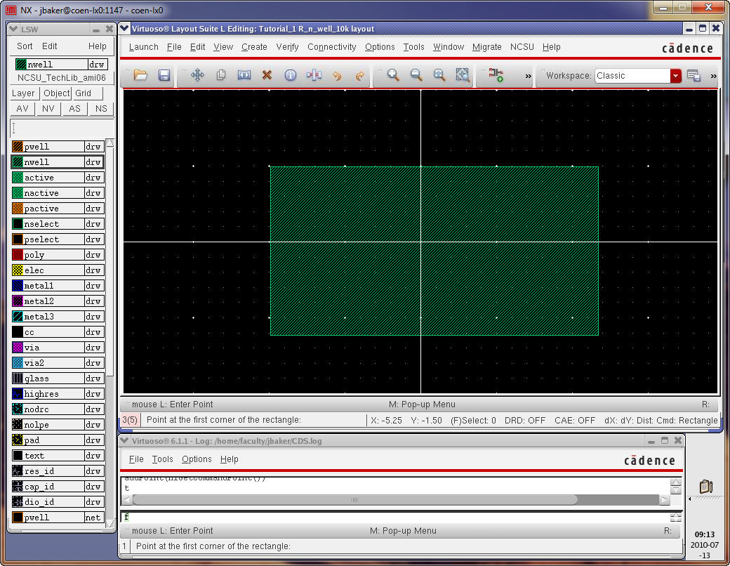
To exit the Create Rectangle mode press Esc (or Virtuoso will continue drawing rectangles).
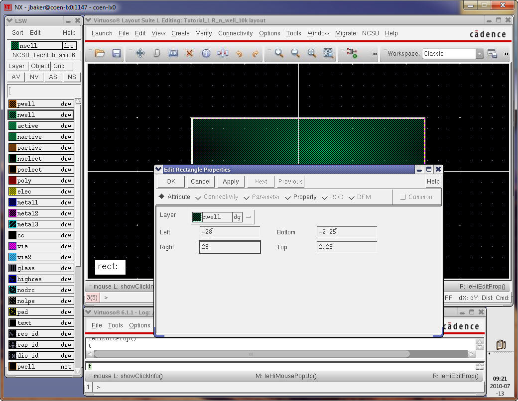
Next select the rectangle and press q (Edit -> Basic -> Properties).
As calculated above we want a resistor that is 56 um long and 4.5 um wide.
After clicking on OK and fitting the layout we get the following.
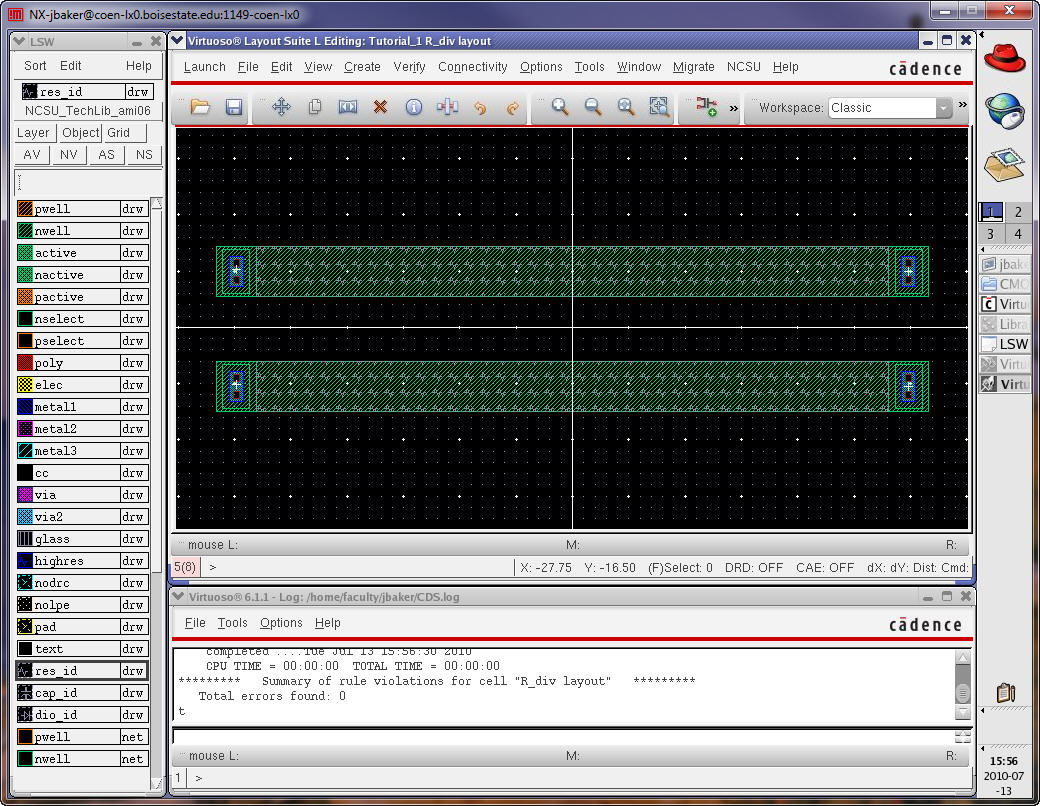
Let’s design rule check (DRC) this layout before continuing.
Using the menu Verify -> DRC the following window pops up.
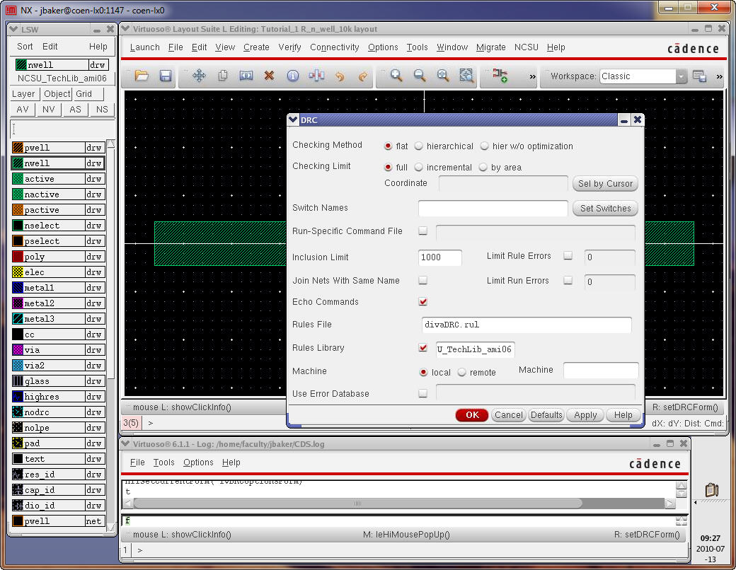
Pressing OK starts the DRC.
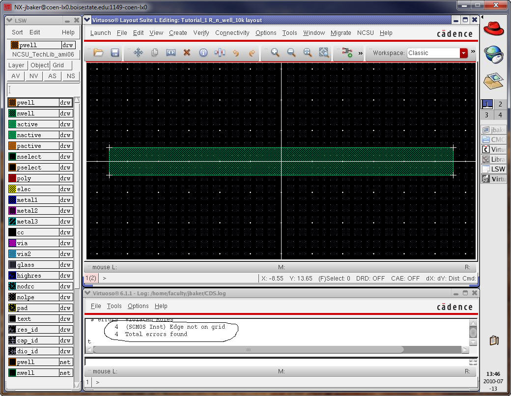
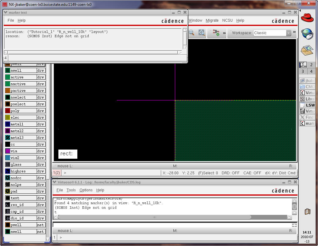
The CIW shows there are 4 errors (the edges are not on grid).
The questions are how do we find out the grid settings and how to view the markers showing the location of the errors (above seeing the markers is easy
since the layout is simple….the crosses in the corners are the markers).
Using the menu Verify -> Markers -> Find Marker (notice you can delete the markers in this menu path too).
Select Zoom To Markers
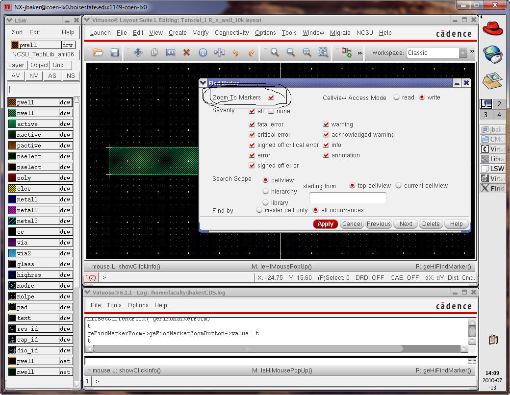
Hitting Apply we get
Close the marker text window, select the layout window, and zoom out a couple of times (press Z) until you can see the grid.
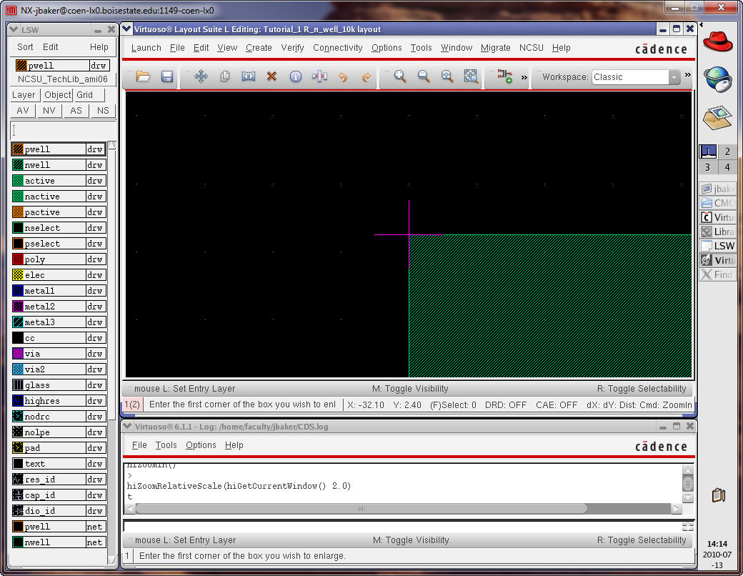
While it’s a little challenging to see in the figure above the corner isn’t snapped to the y-axis grid.
Use Tools -> Create Ruler (or the Bindkey k) to measure the distance between grid points (or just press e, Options -> Display to see
X and Y Snap Spacing is set to 0.15 microns)

The distance between grid points is 1 micron and, as mentioned, the X and Y snapping is 0.15 microns.
Clear the ruler by using the menu items Tools -> Clear All Rulers (or just press K).
Press f to fit the layout in the drawing area.
Use Verify -> Markers -> Delete All followed by OK to delete the markers.
Press Esc a few times to ensure no commands are active.
Next select the layout and press q to get the following
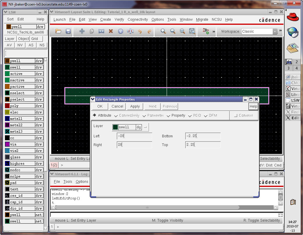
So the length of the resistor is 56 and 56/.15 = 373.3333. To make this a whole number let’s increase the length to 56.1 (so we enter 28.05 in the Left/Right above).
For the width we used 4.5 and 4.5/.15 = 30 so we are okay there.
Running the DRC shows no errors are found.
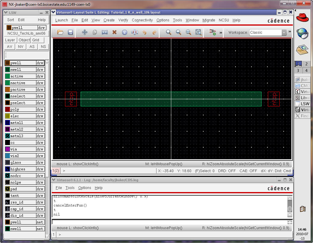
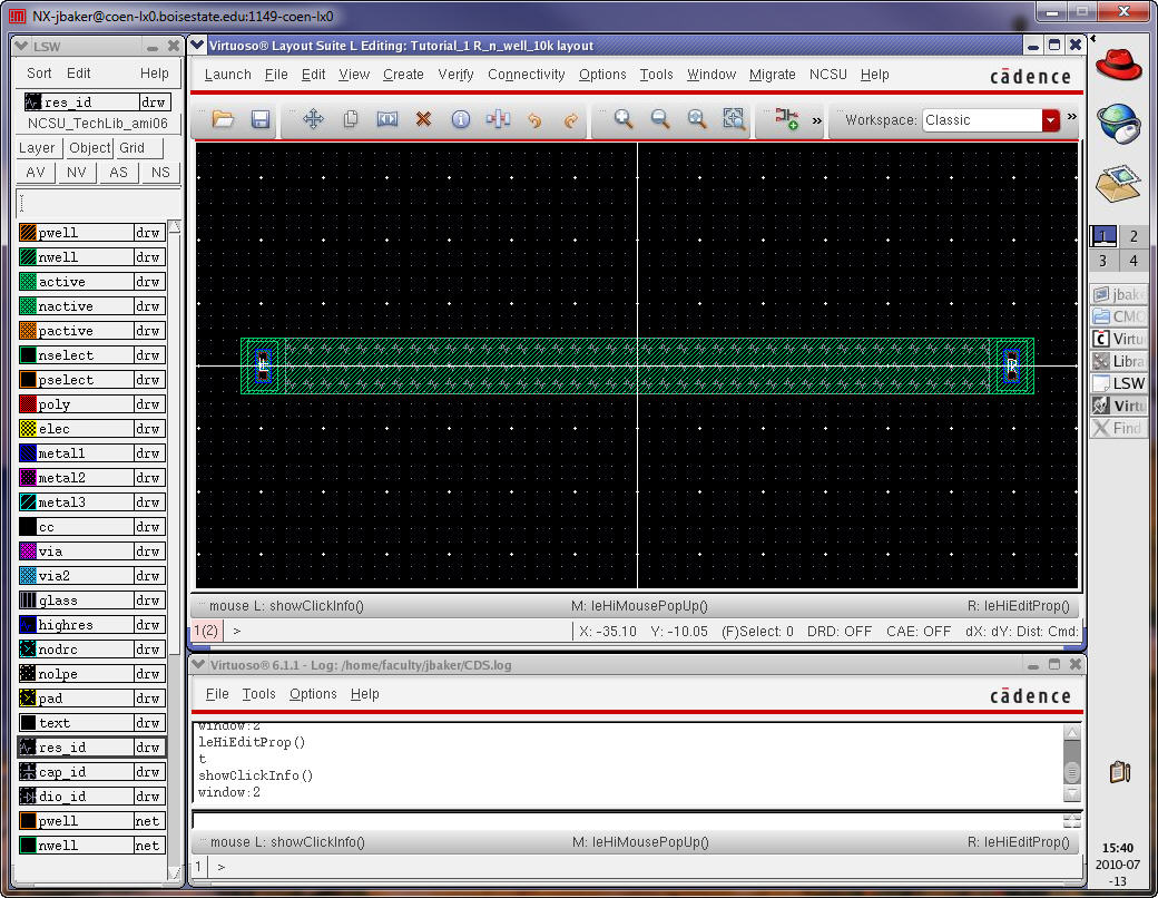
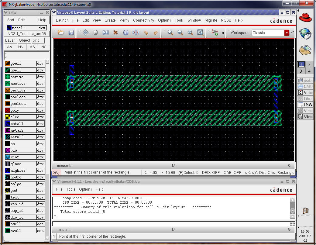
Next let’s add the connections to the ends of the resistors.
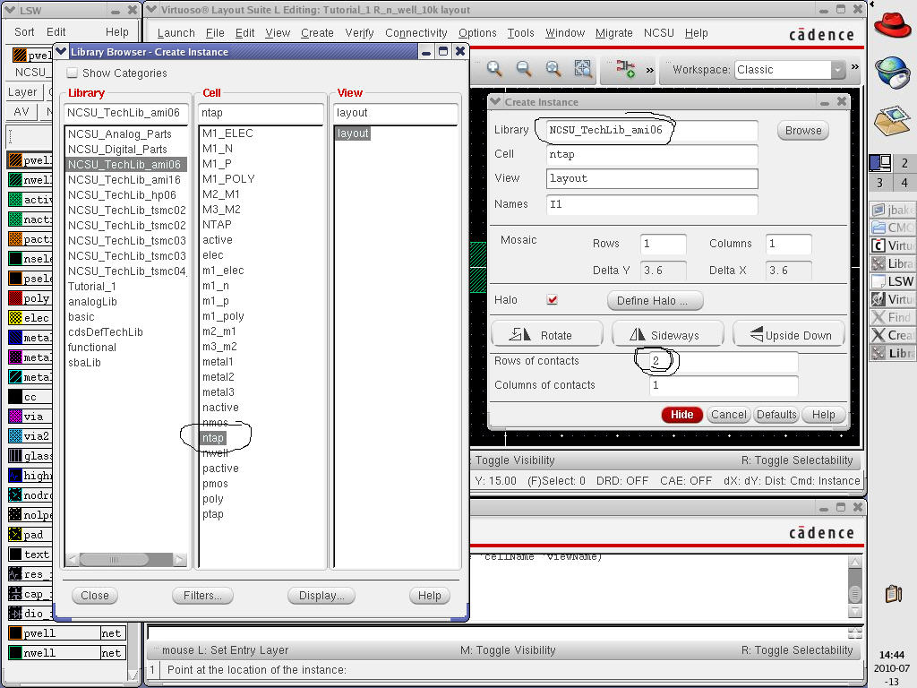
Press i and navigate/select the ntap (metal1 connection to n-well) as seen below.
Adding these connections to the ends of the n-well resistor we get the following.
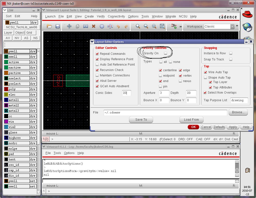
You may have noticed that when placing the nodes they had an affinity to the n-well rectangle. This is called gravity, which can be useful. However,
here it’s not useful so let’s turn it off. Go to Tools -> Editor (or press E) and deselect the “Gravity On” check box.
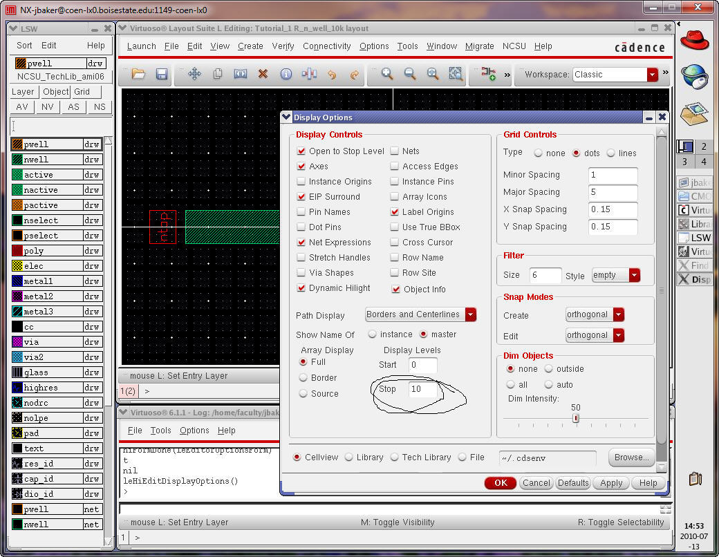
Next notice that the ntap cells are drawn as outlines. Go to Tools -> Display (or just press e) and set the depth of display to 10.
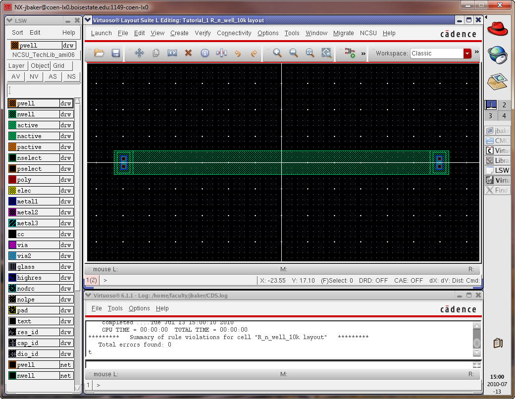
Next select the ntap cells then press m to move them (or use the menu Edit -> Move)
Line the cells up as seen below.
Pressing z then click, move the mouse, then click again to set the window (you can’t click and drag to zoom in).
DRC the layout to ensure no errors.
Next let’s add pins to the layout.
Zoom in on the left side of the layout.
Then use the menu commands Create -> Pin
Select “Display Pin Names”, a name of L (left), and the metal1 layer as seen below.
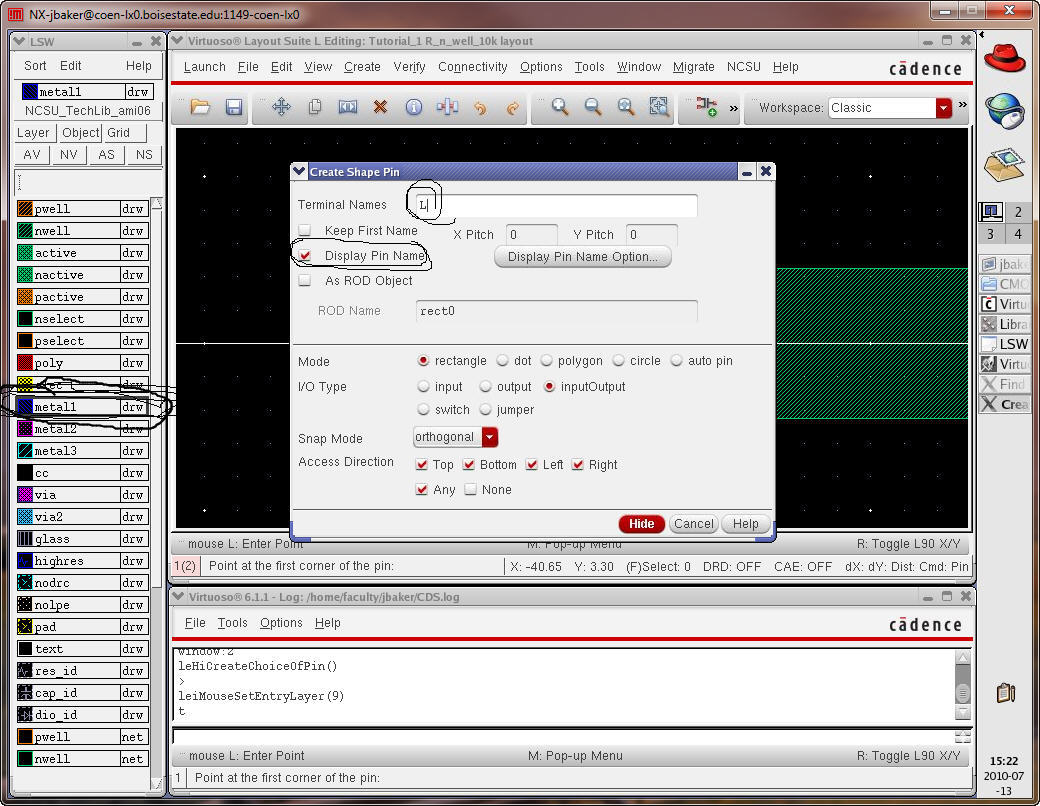
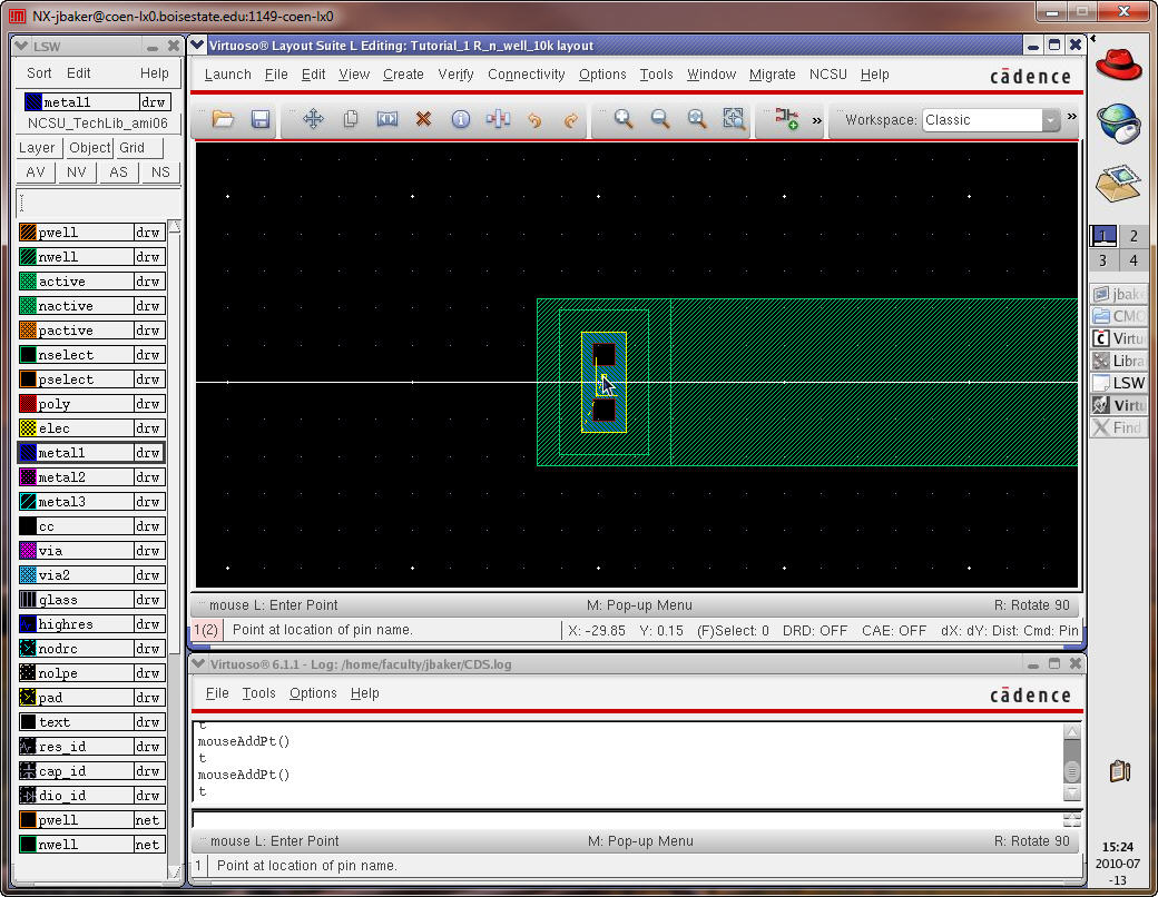
Select Hide and then draw a rectangle around the metal1 on the ntap placing the Pin Name on the center of the metal1 rectangle.
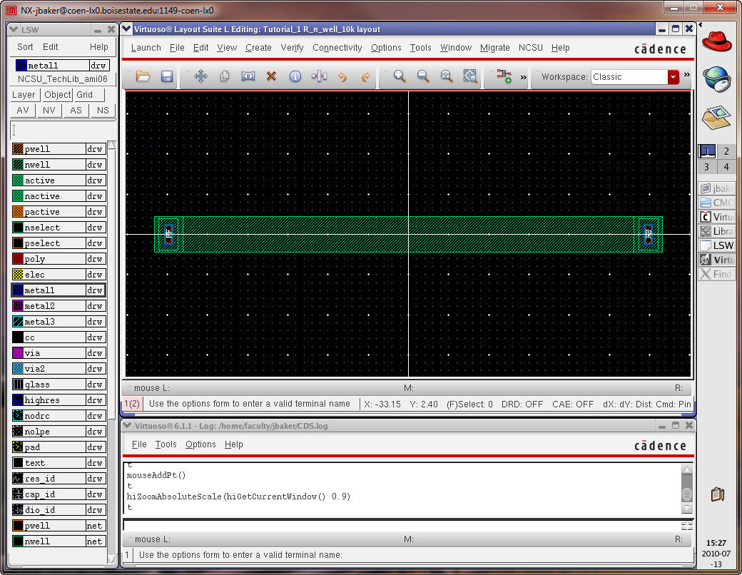
Repeat, but use a Pin Name of R (right), for the other side.
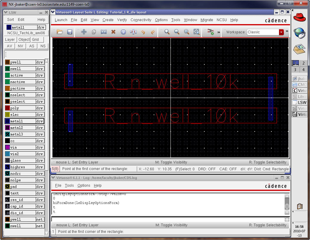
Next select the layer res_id (to identify resistors).
Select r to draw a rectangle.
Zoom in and start drawing a rectangle.
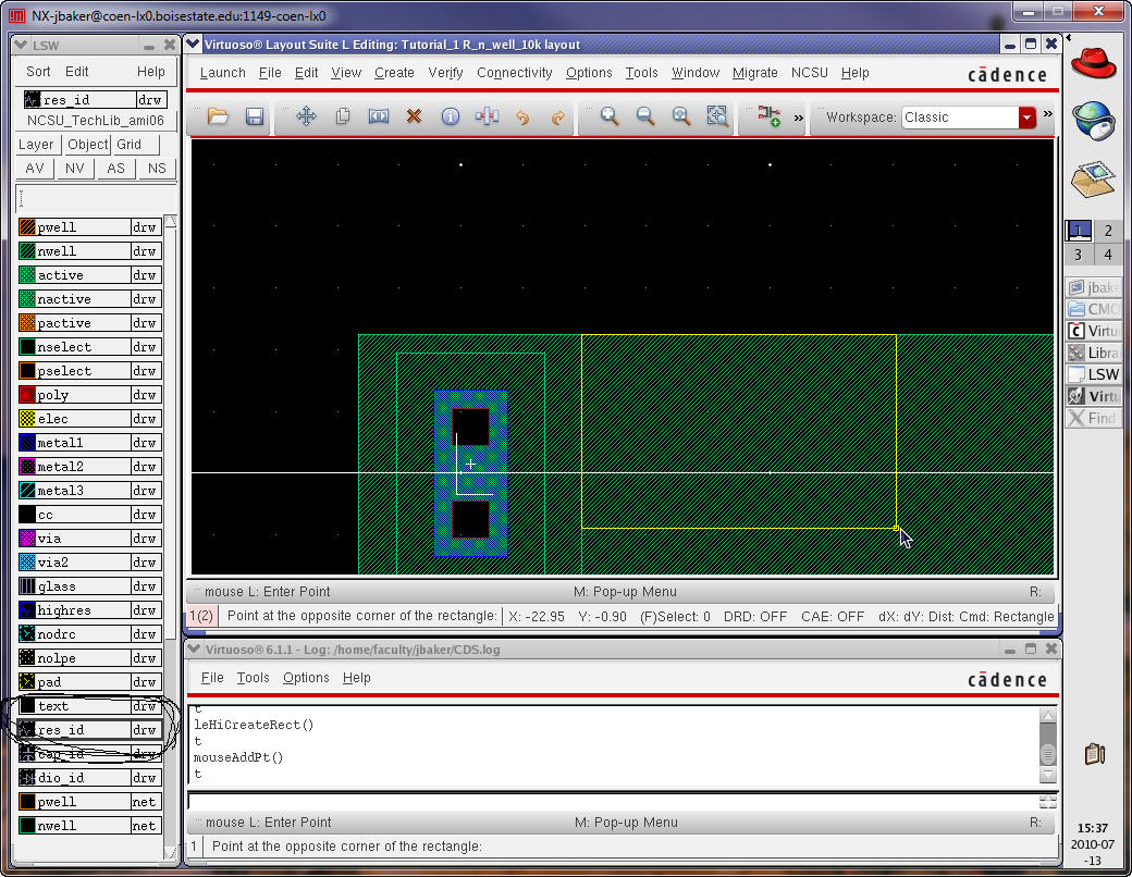
When finished the layout should look like
Next let’s Extract the layout to determine the resistance’s value (and to see if the setups match the 800 ohms n-well sheet resistance we got from MOSIS).
Go to Verify -> Extract
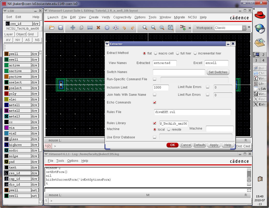
After hitting OK the window closes and an extracted view is created in the R_n_well_10k cell group.
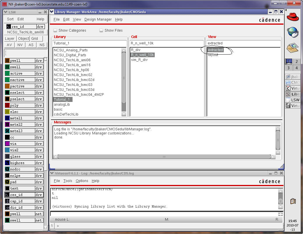
Open this view.
Zoom in to see the resistor’s value is 10.21k.
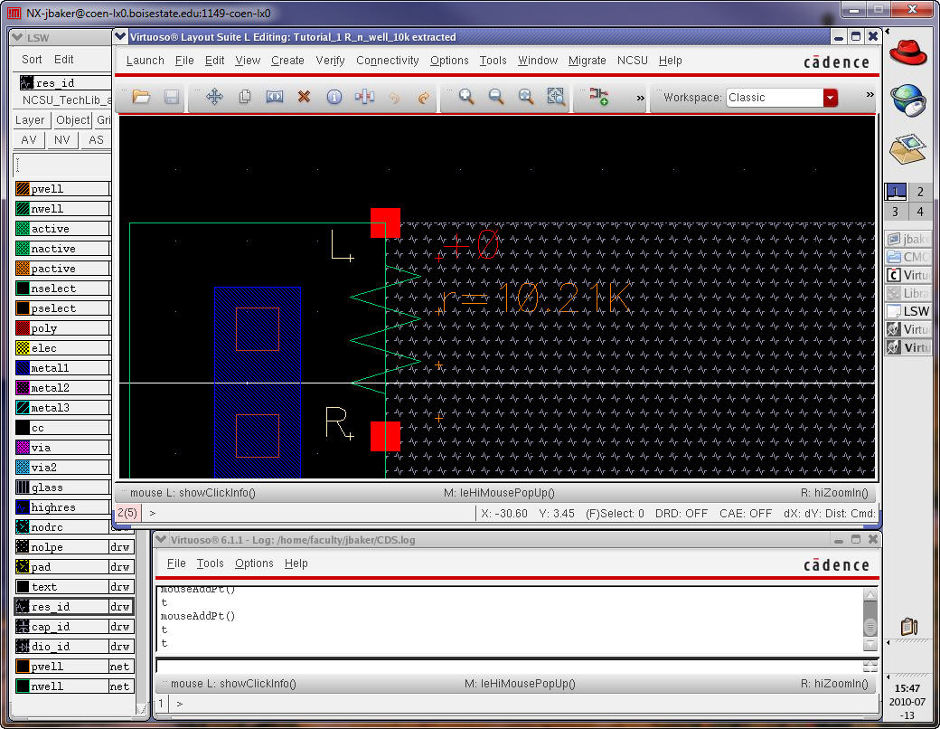
Close the extracted view.
Save and close the layout view of the resistor.
We are now ready to draw the layout of the R_div cell.
Open the schematic view of the R_div cell (so we remember what is in it, like Pin Names).
Open the layout view for the R_div cell (nothing is in this cell).
Instantiate two of the 10k n-well resistor layouts
Remember pressing Esc leaves the instantiate command.
DRC your layout to ensure the resistors are far enough apart.
Next select the metal1 layer in the LSW and add rectangles to connect the resistors together and to connect to the Pins of the resistors.
The rectangles don’t have to overlap the Pins, just touch (abut) the metal1 Pins on the n-well resistors.
(I like to overlap the Pins with metal1.) One example is seen below.
DRC the design to ensure no errors.
Pressing e and set the Stop Depth to zero results in showing the outlines of the cells.
Press e again and set the Stop Depth back to 10. Also ensure, when the Display Options Window is open, that Pin Names is still set to display.
Next add Pins on the metal1 layer named in, out, and gnd. Set the rectangle size of the Pin to the same size as the metal1 seen above.
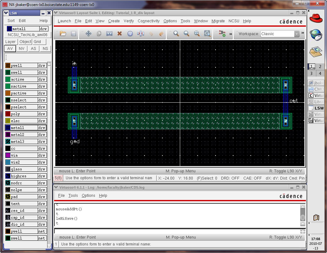
DRC your layout.
Extract your layout (we need to do this before we do a layout versus schematic, LVS)
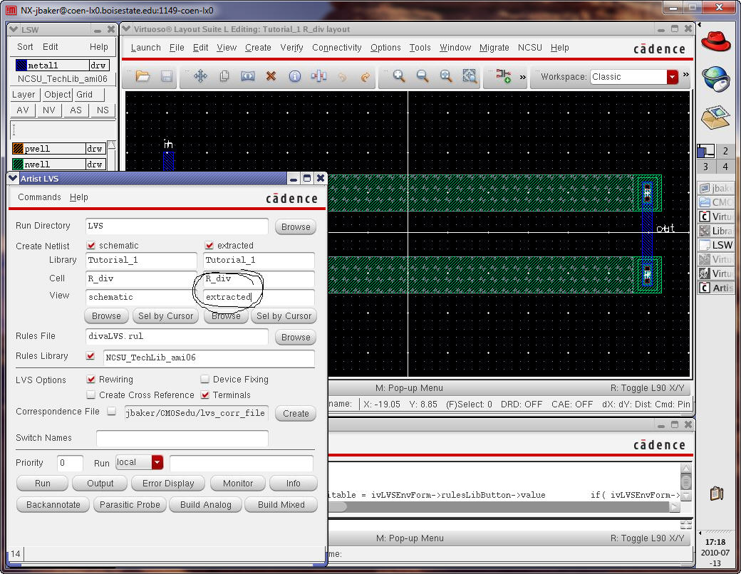
Finally, select Verify -> LVS and set the extracted view’s cell name (here R_div) and that its view is extracted as seen below.
Hit Run and OK to “Save Cellviews” (if asked)
When the LVS is done it will, hopefully, tell you it has succeeded (hit OK).
While the LVS succeeded to run this does not tell us if the layout and schematic match!
After pressing Output above we get the following.
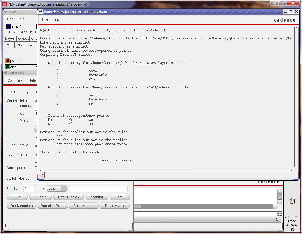
Scrolling down in the si.out file shows the problems.
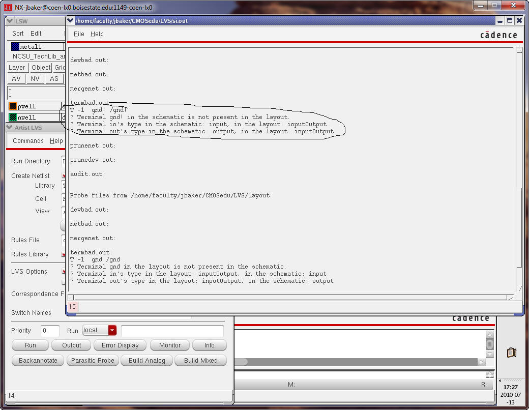
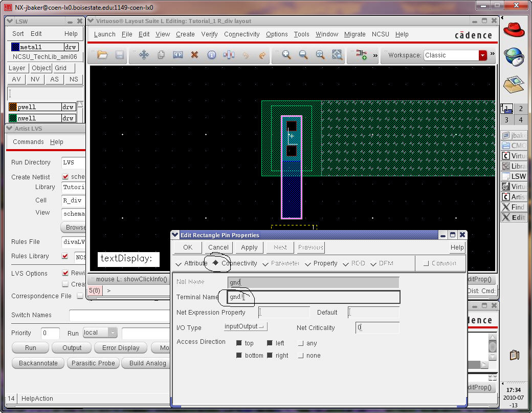
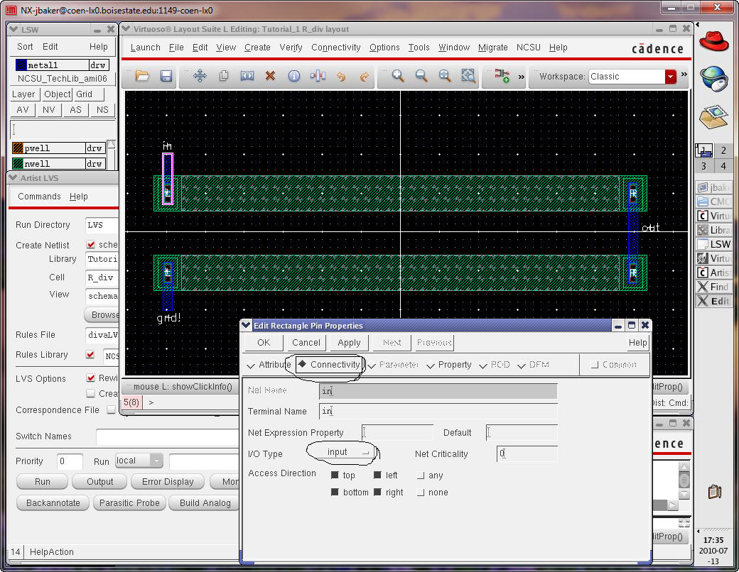
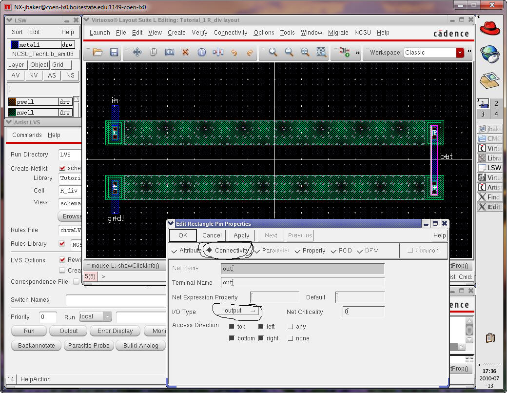
We should have labeled gnd in the layout gnd! (the exclamation point indicates a global value), and our in pin should have characteristics of input (not input/output)
and the out pin should be an output (not input/output).
Note that we could also select the Error Display button above and view the errors in the extracted view (often much easier than viewing text).
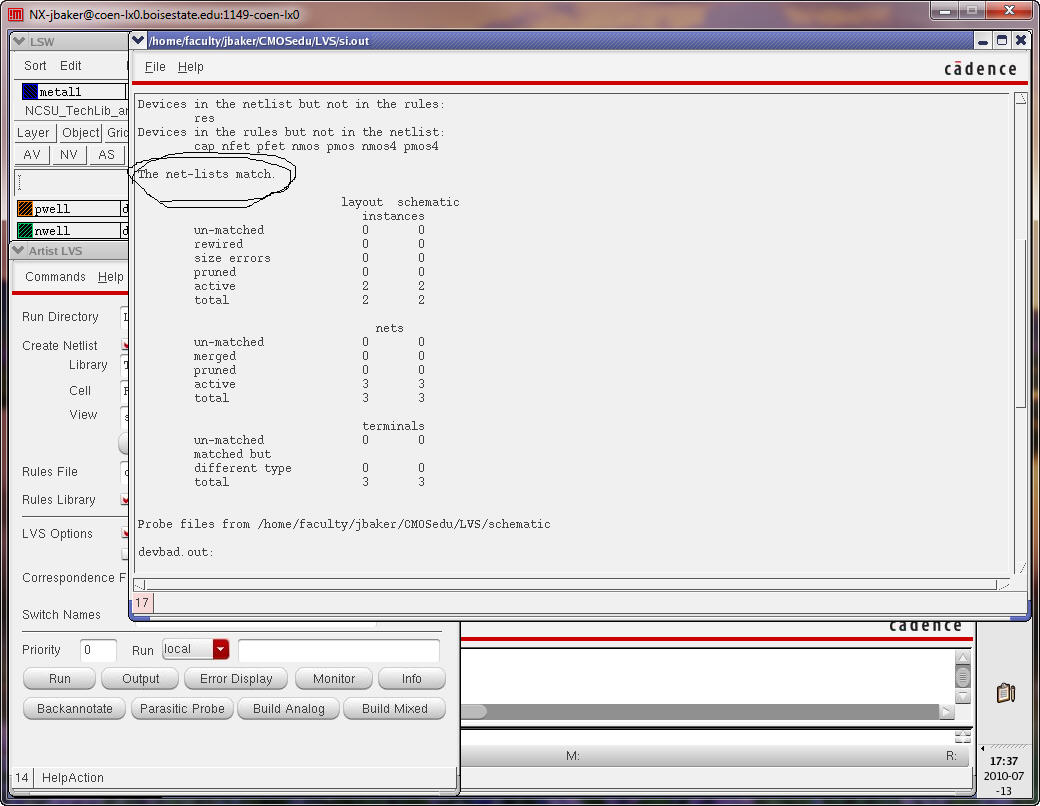
After saving the layout, extracting the layout again, and then running the LVS again we get the following.
This ends our first tutorial.
In this tutorial we’ve covered the fundamental operation of Cadence. Mastering the topics before moving on to the other Tutorials is important.
For your reference the Tutorial_1 directory is available in Tutorial_1.zip.