These are generic design rules. For TSMC02d, you need to use the rule numbers in the DEEP column and multiply the values by λ=0.09μm.
| Rule | Description | Lambda | ||
|---|---|---|---|---|
| SCMOS | SUBM | DEEP | ||
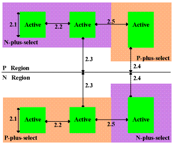
| 2.1 | Minimum width | 3 * | 3 * | 3 |
| 2.2 | Minimum spacing | 3 | 3 | 3 |
| 2.3 | Source/drain active to well edge | 5 | 6 | 6 |
| 2.4 | Substrate/well contact active to well edge | 3 | 3 | 3 |
| 2.5 | Minimum spacing between non-abutting active of different implant. Abutting active ("split-active") is illustrated under Select Layout Rules. | 4 | 4 | 4 |